Synopsys and Ansys power the future of innovation—connecting silicon to systems.
-
-
学生向け無料ソフトウェアにアクセス
Ansysは次世代の技術者を支援します
学生は、世界クラスのシミュレーションソフトウェアに無料でアクセスできます。
-
今すぐAnsysに接続!
未来をデザインする
Ansysに接続して、シミュレーションが次のブレークスルーにどのように貢献できるかを確認してください。
無料トライアル
製品およびサービス
リソースとトレーニング
当社について
Back
製品およびサービス
ANSYS BLOG
June 25, 2020
How to Overcome PCB Modeling Challenges [Updated for 2020]
"Originally published November 2017."
As electronic devices become smaller and more ubiquitous, the printed circuit boards (PCBs) and components that drive them face increasing power densities and evermore complexity. To ensure product reliability and performance, accurate and detailed analysis methodologies are necessary.
Electronics, particularly, can be surprisingly challenging to model. We often think of large bodies (such as cars or airplanes) as the most challenging to simulate. However, simple computers or cellphones can have tens of thousands of bodies with a 1000X range in dimensions (100 microns to 100 mm), leading to highly complex models that require advanced computing capability. A great example is the PCB itself.
PCB Modeling Techniques
The PCB in Figure 1 has 11 structural layers. Five of the layers, laminate or prepreg, are glass fiber-reinforced epoxy with different glass weaves in each layer. Six of the layers consist of thousands of copper traces, pads and planes with epoxy resin (aka, dielectric) filling in gaps between the copper features. Both types of layers have thousands of drilled and plated holes described as vias or microvias.This complex board geometry leads to spatially varying material properties (e.g., modulus of elasticity, density, thermal conductivity, etc.) that must be accurately specified for any type of simulation.
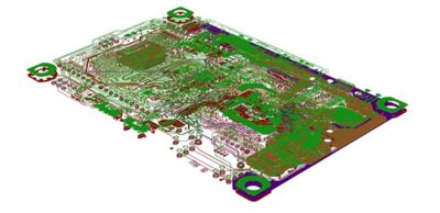
Figure 1: An Ansys Sherlock model of PCB layout geometry
A possible first step in overcoming these PCB modeling challenges is to use Ansys Sherlock. Sherlock is specifically designed to capture and process PCB geometry from any electronic computer-aided design (ECAD) file and can import all industry standard output files, including Gerber, ODB++, IPC-2581 and EDB. As seen in Figure 2, Sherlock can capture all traces, planes, vias, holes, board outlines and stackups. Once the PCB data are uploaded into Sherlock, there are several ways to model the geometry.
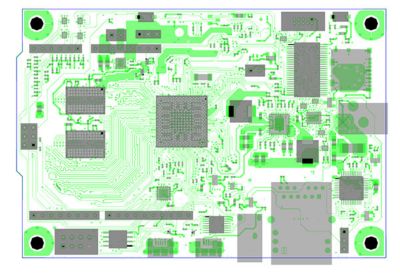
Figure 2: An Ansys Sherlock model of a PCBA top layer
Interested in accurate PCB modeling? Access your Ansys Sherlock Free Trial.
Method 1: Lumped or Effective Material Properties
The most basic approach for dealing with the complex geometry of a PCB is to assume ‘lumped’ or ‘effective’ material properties.
The first step in this method includes calculating the orthotropic properties of the glass-fiber reinforced laminate layers. When viewing the construction details in Figure 1, you will see a variety of glass weaves in different layers (1078, 2116, etc.). Different glass weaves can result in very different material and mechanical behaviors, primarily due to assorted resin content. Elastic moduli (E) and coefficient of thermal expansion (CTE) will vary by more than 40% depending on the laminate construction.
Sherlock can take material properties listed in a laminate datasheet for a standard configuration (50% resin/50% glass) and compute the orthotropic properties for a wide range of glass weaves and reverse out the isotropic properties of the resin.
The next step includes calculating the orthotropic properties of the copper and resin layers. In this method, a percentage copper coverage of each layer of the board is assumed and effective orthotropic material properties can be calculated. Using the board thermal conductivity as an example, the effective thermal conductivity of each layer can be computed as:
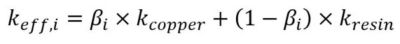
where k is thermal conductivity, βi is the fraction of layer i covered by copper.
The extent to which material properties are lumped can be decided by the analyst. Properties can be lumped across all layers or on a layer-by-layer basis. The lumped approach affords the analyst a reliable first order estimate of board properties but may lead to errors due to the “smearing out” of spatial property variations. Examples of effective properties computed across all layers and on a layer-by-layer basis are shown in Figure 3.
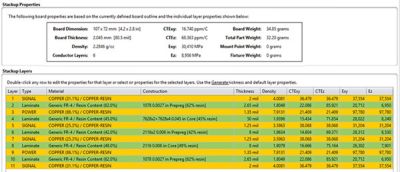
Figure 3: Stackup properties of a PCB in Ansys Sherlock.
The effective properties approach to PCB modeling is great for a first pass assessment, such as pre-layout or on early versions of the layout. However, for final verification additional detail is required.
Watch the “How Much Detail Do You Need When Modeling PCBs” webinar to learn more.
Method 2: Mapped Material Properties (Trace Mapping)
In this approach, a rectangular background grid is constructed on each layer of the board. Each cell of the background grid computes effective orthotropic material properties based on the local concentration of copper and dielectric. This effectively forms a map of the material properties across each layer of the PCB.
The local properties are computed in a manner similar to Method 1. However only a finite section of the board is considered in each cell, enabling the material map to capture local changes in properties. An example of this material map constructed in Ansys Mechanical is shown in Figure 4 below. The mesh in your FEA or CFD model can then reference this underlying material map when determining local material properties of the PCB.
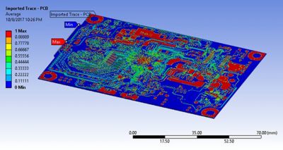
Figure 4: Mapped PCB properties in Ansys Mechanical
The major advantage of trace mapping is the cleanliness of the mesh and the complete control of the mesh density. Without being forced to conform to the complex geometry of the traces, pad and planes, the mesh can consist almost entirely of first-order bricks. Bricks are preferred over first-order tetrahedral elements for structural mechanics modeling as ‘tets’ tend to be too stiff. The preferred element size is between 100 and 500 microns, depending on your application (e.g., thermal, mechanical, thermo-mechanical, etc.). The finer the mesh, the more the trace map starts to correlate to the actual geometry.
Trace mapping enables a more accurate representation of the PCB than the effective properties approach detailed in Method 1. It can also perform a simulation faster and with fewer resources than the approach detailed below, in Method 3.
Due to the increasing complexity of PCB designs, trace modeling is the preferred approach to predict the risk of thermo-mechanical failures.
Method 3: Detailed Geometry (Trace Modeling)
Using a method that lies to the opposite extreme of the simplicity of Method 1, the analyst can choose to represent the entire board explicitly by extracting the full 3D geometry of the PCB layout. In this approach, less assumptions are made as to the distribution of the materials within the board, as each trace and via is modeled in detail.
Because of the growing use of stacked microvias and extremely small traces for high speed circuitry (down to 25-micron widths), there are an increasing number of applications where the failure to include explicit geometry introduces failure risks during manufacturing, verification testing and operation in the field.
However, the challenge of modeling the entire PCB geometry cannot be understated. Not only is the analyst forced into creating a large model (potentially over 1M elements per layer), but the complex geometry is either unable to be meshed or is filled with undesirable element types and aspect ratios.
To overcome these challenges, Sherlock provides users a range of options:
- trace modeling (discussed above)
- trace modeling regions
- trace modeling reinforcements
Trace modeling regions provides the user the ability to create solid geometry for every feature in a pre-defined area. This reduces the potential size of the model and is especially useful when there are thermo-mechanical risks identified with a specific component, such as a ball grid array (BGA) or quad flat pack no lead (QFN). This is similar to the local-global modeling approach, but trace modeling regions creates a local, high-definition model inside of a global, low-definition model.
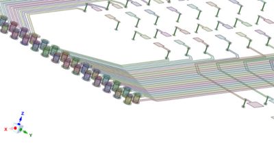
Figure 5: Copper PCB features modeled as shell and beam reinforcements in Ansys Sherlock.
Trace modeling reinforcements is the newest capability available in Sherlock. Reinforcements are 2D or 1D elements that are embedded within 3D structural elements, or mother elements. The strains in the reinforcements are computed from the displacement field of the embedding elements, which implies a strong bond between the reinforcement and the surrounding material (mimicking the bond between copper foil and copper plating and epoxy resin).
The benefit of reinforcements includes a layout geometry that does not influence the mesh of the resin or laminate. This provides the analyst a benefit similar to trace mapping, where the mesh is mostly first-order bricks and there is complete control over the mesh density.
All of these capabilities create exciting opportunities for electrical, thermal, mechanical and reliability modeling of electronics for next generation technologies.