-
-
学生向け無料ソフトウェアにアクセス
Ansysは次世代の技術者を支援します
学生は、世界クラスのシミュレーションソフトウェアに無料でアクセスできます。
-
今すぐAnsysに接続!
未来をデザインする
Ansysに接続して、シミュレーションが次のブレークスルーにどのように貢献できるかを確認してください。
無料トライアル
製品およびサービス
リソースとトレーニング
当社について
Back
製品およびサービス
ANSYS BLOG
August 6, 2021
PCB Design Rules: Wiring and Crosstalk
Today’s electronic devices market demands miniaturized printed circuit boards (PCBs) with a multitude of high-speed functions integrated on a single board. This causes the designers to have traces routed very close to each other to optimize packaging and space. This proximity may cause unintentional coupling of electromagnetic fields, a phenomenon which we know by the name of crosstalk (see Figure 1).
Even though tight packaging may be unavoidable, there are certain PCB design rules pertaining to wiring/routing on a PCB that shouldn’t be violated to avoid potential crosstalk and electromagnetic interference/compatibility (EMI/EMC) issues. We have already gone through some PCB design rules in part 1 of this blog series, but let’s look at some additional important design guidelines in this second and final part. We’ll also look at how Ansys SIwave enables PCB-level simulations to identify areas of potential EMI/EMC issues if and when these guidelines are violated.
(In the following sections, the phrase “critical net” refers to traces on the PCB that may reference high-speed clock/data lines, important sensing lines and so on, depending on the PCB’s application.)
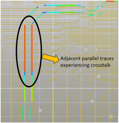
Figure 1: Illustration of adjacent traces on a PCB having potential crosstalk issues.
Rule 1: Critical Net Near I/O Net
It is important to look at the routing of critical nets in relation to the I/O lines because noise is easily coupled on or off the board through these I/O lines leaving or entering the board (see Figure 2) and connecting the PCB to the outside world with other PCBs or modules in the system.
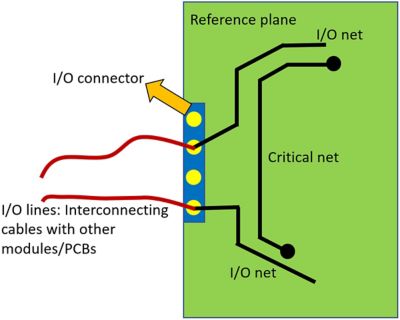
Figure 2: Illustration of a scenario where critical net and I/O net are routed close to each other.
Any noise that enters the board through the I/O lines has the potential to couple to the critical nets carrying important data/clock signals, which would basically be the immunity aspect of the PCB (Figure 3a). In a similar fashion, any high-speed signal being carried by the critical nets can couple to the I/O nets, eventually making its way out to the outside world through the I/O lines coming off of the board and going to other modules in the system. This, in principle, would be the emissions aspect of the PCB (Figure 3b).

Figure 3a (left) and 3b: Potential EMI/EMC issues caused by proximity of critical nets and I/O nets
Rule 2: Exposed Critical Trace Length
On a high-speed PCB (> 100MHz) where wavelengths are shorter, any critical net (see Figure 4a), is electrically long enough to make it an efficient radiator, especially when left exposed on the top or bottom layer. This unwanted radiation can couple to any adjacent trace or even to a cable existing in the component close to the trace. We recommend that the critical nets be buried between the solid planes of the internal layers of the PCB as shown in Figure 4b. This helps to contain the fields from the trace and avoids any unintentional coupling in the form of crosstalk or EMI. If exposing a critical net is unavoidable, keep the length of the exposed part as small as possible. This is because the shorter lengths of the exposed traces would have less tendency to radiate because they will be inefficient antennas if they are electrically small.
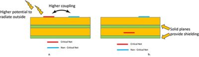
Figure 4a (left) and b: Illustration of having a critical net exposed or buried between solid planes
Rule 3: Critical Differential Net Matching
In theory, a differential pair carries signals that are equal in magnitude and opposite polarity because the EMI generated by the pair cancels out or is negligible. However, this is valid only if the traces in the pair are of equal length and are routed symmetrically close to each other as much as possible. Violation of any of these can create common-mode noise and EMI problems. This is of great concern, especially for differential nets carrying high-frequency critical signals because EMI increases the frequency of the signals being carried. Figure 5 shows a few examples of the correct/incorrect ways of routing a critical differential pair between an IC package and the point of exit on the board (connector).

Figure 5: Return current path in the presence of a split in the reference plane
Critical Differential Net Matching: Simulation and Relation to Actual Test Requirement
In the PCB example in Figure 6a and 6b, we have a simple case of a differential pair routed on a PCB in two different ways: symmetrical and asymmetrical respectively. In both cases, within SIwave they are excited with a differential voltage source on one end and terminated with a load at the other end.
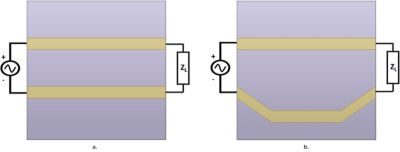
Figure 6a (left) and b: Examples of differential pair routed on a PCB
We run the near field analysis in both cases. In the PCB where the differential pair is routed symmetrically, the near field level is lower than the case where they are not routed symmetrically, as can be seen in Figures 7a and 7b.
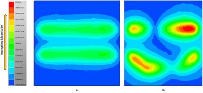
Figure 7a (left) and b: Near field @ 597.45 MHz with symmetric and asymmetric differential pair nets
Let’s say we were to test this PCB against the EMI/EMC regulation AIS 004 (in India) or UNECE R10 (in Europe) radiated emissions requirements. Figure 8 shows a comparative analysis of simulated far field from this PCB at a 1 meter distance in the frequency range 30 MHz ‒1 GHz. Note that an asymmetric differential pair case increases the emission levels by about 8 to 10 dB, also causing the non-compliance at 563.50 MHz and above.
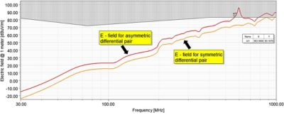
Figure 8: A 1-meter radiated emissions comparison
SIwave’s simulations on the PCB level enable early identification of such EMI issues, which helps to optimize the PCB design before it is passed on for physical testing or even higher level simulations.
To learn more about SIwave, check out the video on our SIwave YouTube channel.