-
-
学生向け無料ソフトウェアにアクセス
Ansysは次世代の技術者を支援します
学生は、世界クラスのシミュレーションソフトウェアに無料でアクセスできます。
-
今すぐAnsysに接続!
未来をデザインする
Ansysに接続して、シミュレーションが次のブレークスルーにどのように貢献できるかを確認してください。
無料トライアル
製品およびサービス
リソースとトレーニング
当社について
Back
製品およびサービス
ANSYS BLOG
September 4, 2018
How to Reduce RFI in the Antenna Design of IoT and Consumer Electronics
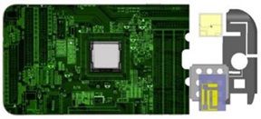
Engineers designing consumer electronics for the internet of things (IoT) do not have it easy. As these devices get smaller they increase the likelihood of radio frequency interference (RFI). These RFI signals could complicate antenna design.
Since there is no unified wireless communication protocol, it seems that every IoT device must be Wi-Fi, Bluetooth, ZigBee and 5G compatible.
Accommodating all these protocols means cramming antennas, transceiver, data source and electrical components into a tiny circuit design.
Each of these components compete for the airwaves within this small space. Even the electronic components that have nothing to do with connectivity could leak out RFI signals.
As the out-of-channel and out-of-technology RFI signals reach a receiver, they could reduce its sensitivity. This is called receiver de-sensitization.
Testing for this interference becomes cost- and time-prohibitive as the number of communication protocols increase and space within the circuit design decreases.
Fortunately, engineers can simulate RFI interference using signal integrity, electromagnetic, circuit and RF system level simulations. These simulations help engineers ensure their high-quality products get to store shelves on time and on budget.
IoT and consumer electronics continue to get smaller. This can cause receiver de-sensitization due to RFI interference.
How to Model RFI in IoT and Consumer Electronics
The first step to modeling RFI is to identify areas within the circuit design that are likely to radiate noise.
This will help engineers to map out where they shouldn’t place receivers.
This simulation can be done using Ansys SIwave and a combination of electromagnetic (EM) solvers.
Engineers can also gain a deeper understanding of the device’s electromagnetic environment and port-to-port coupling using Ansys HFSS.
From here, engineers can characterize the interfering signal at the radio port using a circuit analysis in the time domain. They can then quantify the noise spectra using input/output buffer information specification (IBIS) models.
Finally, engineers can perform RF system-level simulations using Ansys EMIT. This simulation provides a de-sensitization metric to characterize the interference.
By combining all this information, engineers can analyze and mitigate the radio de-sensitization associated with their IoT and consumer electronic designs.
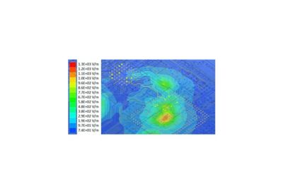
A near-field plot of the printed circuit board (PCB).