Synopsys and Ansys power the future of innovation—connecting silicon to systems.
-
-
Access Free Student Software
Ansys empowers the next generation of engineers
Students get free access to world-class simulation software.
-
Connect with Ansys Now!
Design your future
Connect with Ansys to explore how simulation can power your next breakthrough.
Free Trials
Products & Services
Learn
About
Back
Products & Services
Back
Learn
Ansys empowers the next generation of engineers
Students get free access to world-class simulation software.
Back
About
Design your future
Connect with Ansys to explore how simulation can power your next breakthrough.
Free Trials
TOPIC DETAILS
What is Power Integrity?
Power integrity (PI) is the area of electrical engineering focused on ensuring that an electronic system's power delivery network (PDN) efficiently provides stable power across the system. To operate correctly, printed circuit boards (PCBs), integrated circuits (ICs), and IC packages need electrical power delivered at a consistent voltage with minimal variations over time. It must also not interfere with the signal circuits and lose minimal amounts of energy due to heat generation. Proper power integrity in a design is required to deliver acceptable signal integrity, keep devices operating in acceptable temperature ranges, and minimize power consumption.
Engineers use a variety of software tools and physical testing to assess, modify, and improve the power delivery network, also often referred to as the power distribution network, in electronic systems.
Power integrity is closely related to signal integrity, and engineers usually analyze both at the same time. The importance and challenges of power integrity have increased as electronic systems become smaller, more complex, more demanding of power, and more frequency intensive.
Why is Power Integrity Important?
At first glance, delivering reliable power seems relatively simple compared to the complexities of other areas of electronic circuit design. You connect your device to a power source, set the correct voltage, and then provide power rails to power your signal circuits. However, the reality is more complicated. The movement of electrons generates magnetic fields that can interfere with other circuits or cause power loss due to resistance.
That is why engineers analyze power integrity as early as possible in the design process to identify any potential problems. Delivering the proper voltage range with minimal variation is challenging due to the complexity of modern electronics, which involve multiple components, layers, and interconnects.
But modern electronics are complicated, multicomponent assemblies with multiple layers, vias connecting those layers, and intricate interconnects between components. This geometry transmits both DC power and signals at a wide range of frequencies.
A good way to understand power integrity’s importance is to look at three major types of power integrity problems.
Variations in Power Voltage
An electronics system receives power from an external AC or DC source. Components then convert the input voltage to the desired system DC voltage. However, this power conversion can introduce transient voltage changes that react with the inductance of the PDN, leading to voltage spikes and variations known as noise or voltage ripple.
Another source of voltage fluctuation is rapid changes in current demand. Transistors switching from their static current to a higher voltage, usually on a clock signal, is the most common cause of dynamic current. The voltage regulator module (VRM) in a device’s PDN can’t respond immediately to the change in current, which can cause the voltage to spike or drop (known as voltage ripple). A good example is a microprocessor shifting from an idle state to heavy computation and then back to idle, causing significant power fluctuations. This jitter can affect both the power supply and return paths of the PDN.
Electromagnetic Interference (EMI)
Any change in the power or ground voltage can create electromagnetic waves that can induce unwanted current into the surrounding circuitry. Likewise, signals produced by high-frequency digital or AC circuits can induce unwanted current into the power circuit. This crosstalk, or electromagnetic coupling, has a direct impact on signal integrity. If engineers don’t find and eliminate this crosstalk early in the design phase, it may arise in later required electromagnetic compatibility (EMC) testing. If not caught there, it will result in signal integrity issues during operation.
Power Loss
Insufficient conductivity in the power circuitry can lead to voltage drops in the PDN. When an electrical current encounters resistance, power is lost as heat generation. That is why PCB and IC package design must ensure that the power planes, power vias, and return path configurations have low impedance and resistance.
Overcoming these and other power integrity issues is integral to defining today's high-speed designs that deliver the high-performance electronic systems powering our modern world. Without proper power integrity, products can overheat or suffer signal integrity problems, resulting in poor performance or even component failure.
What are the Key Factors in Power Integrity?
The PDN in an electronic system consists of the conducting paths and component configuration in the PCB layout or IC package. The PDN must both deliver current from the power source and return current via a low-impedance return path. Engineers seeking to understand power integrity should consider the following key factors in PDN performance:
Power Rail
The conductive path that distributes a specific voltage to circuit components is called a power rail. In PCB design, this refers to the conductive path that distributes power to different layers on the board and then back to ground. The term “rail” comes from early analog electrical designs, in which the power source was an actual conductive metal rail.
Power Planes
PCBs, which include flexible PCBs, are made up of alternating material layers of conductive or insulating materials. Vertical, hollow conducting columns called vias connect the different conducting layers in the stackup. The layers that provide power to the signal-processing layers are called power planes. Because the layer thickness is fixed, the current-carrying capacity of the conducting material on the power planes is determined by the width of the conductive traces. If they are not wide enough, localized resistance can create power loss due to Joule heating.
Return Path and Ground Planes
To complete a power circuit, current must return from the signal circuits to the power source. The return path is the part of the PDN that enables current to flow back from the load to ground. In a PCB, the layers that make up the return path are called ground planes.
Interconnect
Interconnects are the connecting components between different portions of an electronic system. They can take the form of PCBs, ball grid arrays, or pins. Because interconnects carry signals and power between components, they are susceptible to power integrity issues.
Ground Bounce
Ground bounce is a phenomenon in which the ground voltage temporarily “bounces” from its expected constant value. EMI produced by current fluctuations from rapid voltage changes in the signal circuit induces unwanted current in the ground plane, causing ground bounce. Parasitic capacitance in PCB traces and vias can also contribute to ground bounce when they store and release charge during switching.
Jitter
Jitter refers to variations and spikes in the digital signal caused by noise in the PDN, EMI from signal and power circuits, timing issues, and component variability. Because jitter is a major contributor to signal integrity problems, reducing it is an important part of board design. For power integrity, engineers minimize jitter by reducing variability in power and ground voltages as well as reducing inductive coupling between power and signal circuits.
Parasitic Losses
This refers to any power loss in an electrical circuit due to energy transfer that doesn’t contribute to the function or output of the circuit. In a power integrity context, this includes power loss due to capacitive, inductive, and resistive effects. Parasitic losses not only reduce circuit efficiency, but they can also cause unwanted heat that impacts performance and physical robustness. In addition to power integrity, parasitic losses also impact signal integrity.
Joule Heating
When current encounters resistance in a material, some electrical energy is converted to thermal energy. This process is called Joule heating, named after the physicist James Prescott Joule. The amount of heat energy generated is directly proportional to the material's resistance and the mathematical square of the current.
PDN Impedance
PDN impedance is the opposition to current flow in a PDN due to resistance, inductance, and capacitance. The ultimate goal of power integrity design is to maintain PDN impedance that is lower than the system’s target impedance. Target impedance is frequency dependent and varies greatly, from less than 1 mΩ at DC to under 100 mΩ at 10 GHz. A PCB’s layout influences PDN impedance, the inductance of current paths, and the capacitance between power planes and traces on signal layers. Decoupling capacitors can also affect impedance. PDN impedance can vary significantly across frequency ranges.
Decoupling Capacitors
Decoupling capacitors are discrete components that provide current when the voltage regulator module (VRM) can’t respond quickly enough. Because the PDN impedance varies across frequency ranges, designers place multiple decoupling capacitors in the PDN to maintain low impedance across frequency ranges.
How is Power Integrity Measured and Analyzed?
Once engineers have designed a power distribution network, they must measure and analyze the voltage and temperature over time on both the power and ground sides. This can be done virtually with simulation software by using physical analysis tools such as a digital voltmeter or oscilloscopes. Regardless of the approach, the goal is to identify causes of power integrity issues: jitter, EMI, and Joule heating.

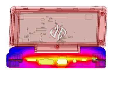
Side-by-side comparison of heat caused by power integrity issues captured with a thermal camera (left) and simulated in Ansys Icepak software (right)
For thermal issues, engineers examine heat maps of the system taken by thermal cameras and simulated temperature contours. Jitter, EMI, and resulting impact on signal integrity are measured and analyzed as voltage over time at points in power and ground circuits and as eye diagrams in signal circuits.
Measuring and Analyzing Power Integrity Using Simulation
Once the PCB or IC package design is finished, engineering teams should begin evaluating power integrity using a digital model. Because it depends so strongly on geometry, simulating the electro-thermal design of the PDN is a good starting point. First, team members should simulate the operating case with the system’s highest power demand and calculate the voltage drop across the power and ground planes.
Multiple multiphysics simulations that involve different variables may be necessary in modeling heat transfer. Engineers must ensure that their thermal simulation uses realistic environmental conditions representing worst-case operating conditions. Based on the simulation results, engineers can change the power and ground circuit geometry, add or move thermal vias, and apply electronics thermal management best practices to spread and control heat.
When coupled with Ansys SIwave software, Ansys Icepak software is an effective tool for this type of analysis. It can read geometry directly from ECAD software and simulate current flow and power dissipation. After that, heat flux data can be passed to Icepak software to calculate and update the temperatures in the electromagnetic model.
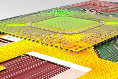
An image from Ansys SIwave software showing power loss in an electronic assembly with the chip package and PCB. Engineers use this information to modify geometry to decrease losses and ensure power integrity.
Once a power loss design is chosen, the next step should be simulating electromagnetic interference coupled with PDN noise analysis. By solving for EMI in multiple operating conditions, engineers can measure signal and power integrity simultaneously. A comprehensive tool like SIwave software enables you to use the same power loss model when simulating capacitive and inductive coupling.
First, engineers must measure the PDN impedance and fine-tune the design until it meets the target impedance. These iterations may involve introducing spacing between circuit traces, modifying power or ground plane geometry, moving or adding vias, or introducing capacitors to reduce crosstalk.
Most electronics systems include both PCBs and integrated circuits. That is why engineers need a robust set of tools to calculate power integrity at the chip level, such as the Ansys Totem platform for analog and mixed-signal ICs or the Ansys RedHawk-SC platform for digital and 3D-ICs.
The most important part of virtual measurement and analysis is ensuring that the simulation accounts for all real-world operating conditions and usage scenarios to make sure all potential power integrity issues are identified and resolved.
Physical Power Integrity Measurement and Analysis
Even after extensive simulation and power integrity signoff, most design processes still require physical testing. The measurements and analysis needed on the test bench are similar to those used in simulation. Engineers or technicians place probes at critical locations on the PCB to capture the voltage over time. Oscilloscopes can then use this data to produce eye diagrams that compare input and output signals.
In addition, the use of thermal cameras or thermocouples to monitor temperature change over time is a necessary part of physical testing. As in the digital environment, the device should be subjected to many different environmental conditions and usage scenarios to ensure reliable performance.
Related Resources
Let’s Get Started
If you're facing engineering challenges, our team is here to assist. With a wealth of experience and a commitment to innovation, we invite you to reach out to us. Let's collaborate to turn your engineering obstacles into opportunities for growth and success. Contact us today to start the conversation.