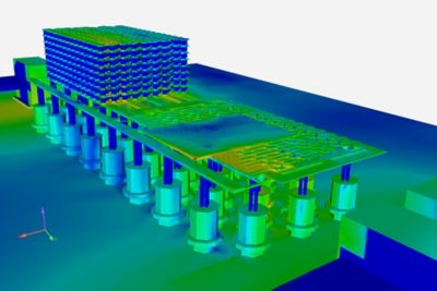
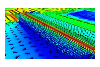
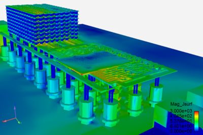
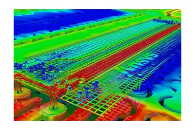
Next‑generation chip‑package systems face increasingly complex power‑delivery demands — tighter integration, higher current density, advanced 3D packaging (InFO, CoWoS, WoW), and ultra‑dense PDNs that strain the limits of traditional 2.5D and reduced‑order tools. These architectures require accurate broadband modelling across dies, packages, RDLs, and boards to reliably predict IR drop, impedance, resonances, and coupling paths.
HFSS‑PI delivers the industry’s first high‑capacity, broadband 3D Power Integrity solver purpose‑built for these challenges. Powered by the NexGen HFSS Prism mesh‑and‑solve technology, it enables end‑to‑end PDN modelling with true 3D EM accuracy — from DC through high frequencies — while scaling to massive multilayer designs. This allows engineers to confidently analyze coupling mechanisms, return‑path behaviour, and power‑delivery bottlenecks earlier and with far greater fidelity than legacy tools.