-
-
Access Free Student Software
Ansys empowers the next generation of engineers
Students get free access to world-class simulation software.
-
Connect with Ansys Now!
Design your future
Connect with Ansys to explore how simulation can power your next breakthrough.
Countries & Regions
Free Trials
Products & Services
Learn
About
Back
Products & Services
Back
Learn
Ansys empowers the next generation of engineers
Students get free access to world-class simulation software.
Back
About
Design your future
Connect with Ansys to explore how simulation can power your next breakthrough.
Free Trials

Ultra-large analog and mixed-signal chips are advanced integrated circuits (ICs) that seamlessly combine analog and digital components on a single semiconductor chip. These innovative mixed-signal ICs facilitate smooth interaction between the two, significantly enhancing overall chip performance and functionality.
Most analog and mixed-signal (AMS) semiconductor designs are relatively small when compared to the larger digital chips now being manufactured for AI and graphics processing. Digital chips can easily grow to contain more than a billion transistors on a single chip, while AMS chips often contain only several thousand. The reasons for this discrepancy stem from complex multiphysics interactions that influence analog circuit behavior.
Analog effects are often highly nonlinear and extremely sensitive to the precise details of the physical layout. Critical electrical parameters like inductance can even be influenced by current flows far away on the chip. Chip engineers, as well as simulation tools, struggle to simulate and understand this complexity, which naturally limits the size of analog circuits.
Analog engineers rely on electronic design automation (EDA) software tools to design their chips, yet these tools have also typically been limited in their capacity. This is because it is difficult to scale up analog simulation engines, like electromagnetic analysis, beyond a certain level.
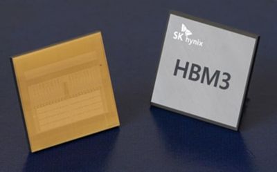
HBM3 high-bandwidth memory from SK Hynix with 12 memories in a 3D stack. Photo courtesy of SK Hynix
Advanced Manufacturing Fuels a Need for Analog Solutions
The AMS landscape has undergone a lot of evolution in the past few years, leading to the emergence of very large semiconductor devices that need fully analog analysis. Examples of these include high-bandwidth memories (HBMs) like HBM4, field-programmable gate arrays (FPGAs) on advanced manufacturing nodes, and complementary metal-oxide-semiconductor (CMOS) image sensors (CIS). In addition, the entire semiconductor industry is embracing 2.5D (side-by-side) and 3D (stacked) multi-die assembly technology. The dozen or more chips in these enormous semiconductor systems are wired together through large connectivity substrates called interposers.
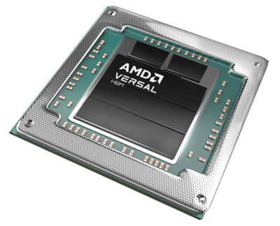
Versal field programmable gate array (FPGA) from AMD with integrated high-bandwidth memory module (HBM). Photo courtesy of AMD
Many of these designs are digital in name, but they may in fact require extensive analog simulation to achieve reliable success. They are also very large — an HBM4 memory module commonly used in high-performance computing (HPC) applications has more than 64 billion transistors. The largest FPGAs used for low-volume industrial applications contain more than 40 billion transistors. CMOS image sensors used in digital cameras and smartphones are some of the most advanced 3D-IC multiphysics stacks on the market, containing more than 10 million pixels. And interposers that connect the many chips in a 3D-IC assembly contain millions of signal lines.
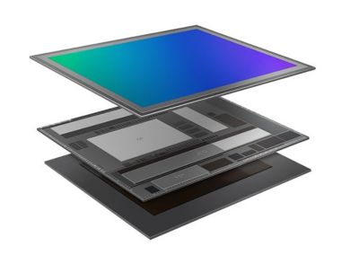
An ISOCELL CMOS image sensor (CIS) from Samsung showing an image sensing chip stacked on top of a data processing chip. Photo courtesy of Samsung
The reasons for this evolution are rooted in powerful market trends. Advanced manufacturing nodes enable very high-frequency digital signals that bring fresh challenges to analog designs. These cannot be accurately simulated with traditional resistance-capacitance (RC) modeling. At these speeds, full electromagnetic modeling, including inductance (L) and shielding metal, becomes essential — and that requires analog simulation tools.

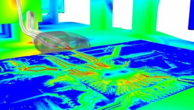
Ansys HFSS electromagnetic simulation results of the interposer for a 3D-IC multi-die assembly
Another driving trend is the pervasive use of video in today’s devices, which has placed a premium on high-definition image sensors. These devices also rely on analog analyses to support optics applications, charge-coupled devices (CCDs) used in digital imaging, and high-speed inputs/outputs (IOs). The programmable logic and high-speed connectivity available with FPGAs are also examples of nominally digital circuits that are analyzed with analog tools. Embedded memories, HBM, CIS, and FPGA are all very large designs with millions of transistors that far exceed the size of traditional AMS chips.
New Tools for a New Era of Analog Design
Designers of large circuits need a new generation of analog tools that can reliably predict analog behavior at high speeds and with advanced nodes. Traditional methods previously involved only analyzing small subsections, but these mega-designs require full-chip simulation for reliable accuracy. Ansys has collaborated closely with some of the world’s foremost silicon vendors to develop tools and technology that address these challenges.
The first technology thread involves radically increasing the speed and capacity of foundational simulation algorithms. Popular electromagnetic tools like Ansys HFSS chip-to-system electromagnetic simulation platform and Ansys RaptorX silicon-optimized electromagnetic solver now feature sophisticated mesh fusion technology to quickly simulate large models with hundreds of connection ports in a single pass, with no loss in accuracy.
Another emerging analog challenge facing designers is verifying electrostatic discharge (ESD) circuitry across multiple connected chips on a 3D-IC. Ansys has developed the Ansys PathFinder-SC electrostatic discharge reliability signoff platform for large IPs and 3D-ICs, which was certified by TSMC foundry as a solution for multi-die ESD signoff. Power integrity and voltage drop analysis have also become increasingly computationally intensive as designs grow larger. The Ansys Totem-SC power integrity signoff platform for large analog, mixed-signal, and 3D-ICs is a targeted design solution for ultra-large AMS designs.
Secondly, Ansys has worked closely with major foundries to fully support layout-dependent effects (LDEs) that emerge when designing with advanced finFET nodes at 10 nm and below. This is essential in accurately predicting capacitance and inductance at these advanced nodes, which can show deviations of 25% or more due to LDE. Large AMS designs are manufactured with these advanced processes because they are the only ones with the required integration density to create millions of transistors in a large design.
Thirdly, Ansys has shifted many of its core algorithms into modern, cloud-optimized data infrastructures that use big-data analytics techniques for electronic simulation. With a naturally distributed data organization, analog power integrity tools like Totem-SC software can be run in the cloud to analyze eight memory chips in an HBM4 stack in under 24 hours with 250 compute cores. This is radically beyond the capabilities of legacy analog EDA tools and provides much-needed simulation capabilities to design engineers operating at the leading edge of AMS design.
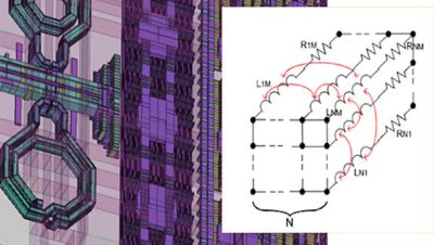
Accurately capturing the behavior of high-speed signals requires full electromagnetic analysis of the interconnect, including parasitic inductance (L) as well as parasitic resistance (R) and capacitance (C).
Analog simulation of a complete chip package and connector with HFSS software using mesh fusion technology. Mesh fusion radically increases the speed and capacity of HFSS software without impacting accuracy.
Address High-capacity Challenges With Simulation
The trend of using more advanced nodes to design increasingly large AMS circuits continues in products like embedded memories, HBM, image sensors, FPGAs, and 3D-IC interposers. Traditional analog design tools have provided neither the data infrastructure nor the algorithmic power necessary to analyze such large designs. Stepping up to this challenge, Ansys’ high-capacity design software tools enable analog engineers to accurately simulate the behavior of some of the largest AMS designs in the industry to deliver high-performance products on schedule and on spec.
Download the Optimizing Analog Design with Multiphysics e-book and learn more about how you can solve your analog design challenges with Ansys solutions.
Just for you. We have some additional resources you may enjoy.


The Advantage Blog
The Ansys Advantage blog, featuring contributions from Ansys and other technology experts, keeps you updated on how Ansys simulation is powering innovation that drives human advancement.