-
-
Access Free Student Software
Ansys empowers the next generation of engineers
Students get free access to world-class simulation software.
-
Connect with Ansys Now!
Design your future
Connect with Ansys to explore how simulation can power your next breakthrough.
Countries & Regions
Free Trials
Products & Services
Learn
About
Back
Products & Services
Back
Learn
Ansys empowers the next generation of engineers
Students get free access to world-class simulation software.
Back
About
Design your future
Connect with Ansys to explore how simulation can power your next breakthrough.
Free Trials

Imagine trying to keep your phone running smoothly while it juggles maps, music, and messages — all at once. Now, imagine designing the tiny electrical highways inside your phone to handle those tasks without causing overheating or wasting energy. This is the challenge semiconductor engineers face every day, especially when it comes to power devices. These components are the unsung heroes behind everything from your smartphone to electric vehicles. Simplifying and speeding up the complex job of designing and testing these devices is a daunting task, but it is one that is rapidly advancing thanks to simulation.
Design Challenges in Power Devices
Power semiconductor devices are a core element of power management systems that control the voltage (V) and current (I) supplied to other electronic devices, circuits, and systems. The number of power management designs has exploded due to the rapid growth in applications that depend on them: mobile devices, datacenters, artificial intelligence (AI) systems, and electric vehicles, to name a few. For example, the cell phone in your pocket contains many power devices in its power management integrated circuits (PMIC), voltage converters, and audio amplifiers.
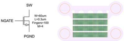
Low-side powerFET schematic (left) and low-side powerFET layout (right).
The most popular power device type is a metal-oxide-semiconductor field-effect transistor (MOSFET), although other device types like bipolar transistors, diodes, and resistors are also used. Power MOSFETs (also called powerFETs) are manufactured in a wide array of semiconductor technologies from mature processes to the latest subnanometer nodes. They are designed for voltages as low as 1 V to as high as thousands of volts.
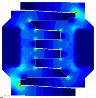
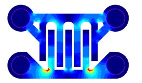
Analysis of a power MOSFET showing the distribution of the current flow
Power devices are designed and manufactured in different forms, including as discrete elements, integrated in dedicated PMIC circuits, and embedded as part of a larger system-on-chip (SoC) design.
Power devices look deceptively simple as a single MOSFET instance. However, to achieve low resistance — in the range of 1-100 milliohms (mΩ) — it must have a very wide gate and a large surface area. Just one power MOSFET gate can take up several square millimeters of silicon, with a total gate width of up to 10 m spread across hundreds of fingers, or narrow, parallel gate segments.
Power device designs must satisfy many requirements, including:
- Low parasitic series resistance for source and drain paths to improve efficiency
- Uniform current distribution over the device surface to ensure consistent performance
- Avoidance of current “hotspots” that may lead to electromigration and damage from self-heating
- Low parasitic inductance in the circuit paths to support stable switching
- Efficient connection to the package and printed circuit board (PCB)
- Efficient surface area utilization
- Optimal use of available metal wiring layers, which carry current across the chip
- Controlled switching characteristics to prevent overshoot, ringing, or unwanted noise
- Avoidance of shoot-through current, which is a brief current surge that turns on both MOSFETs and wastes power and generates heat
- Reliable electrical connection to the transistor’s bulk region to maintain consistent device operation
The total drain-to-source resistance of the power MOSFET when switched on (RDSon) is a critical parameter on most power devices, as it determines the efficiency and amount of power lost in the device. In advanced processes, RDSon can involve more than 15 layers of interconnect metal, and getting it right can take a substantial amount of engineering time.
Current density is another important design parameter. When too much current flows through a wire, it can induce an effect called electromigration. Electromigration physically moves metal atoms over time, creating weaknesses that can lead to premature device failure. A high current density also causes local self-heating, which makes the reliability problems even worse.
With those parameters and others, designing the layout of a power device can feel like an art form, in which careful attention to detail is needed to create a high-quality result.
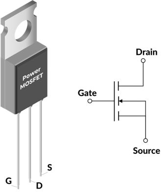
A discrete power MOSFET is shown in a package with three leads for gate, drain, and source, and its corresponding schematic symbol.
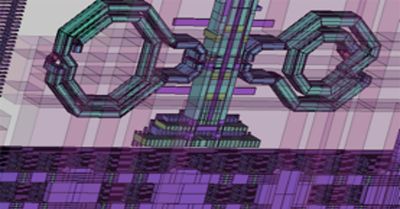
Many IC design groups have dedicated teams of layout engineers specifically focused on constructing power devices. Days, weeks, and even months go into the development and simulation of large power devices with their complex 2D shapes on the top interconnect layers.
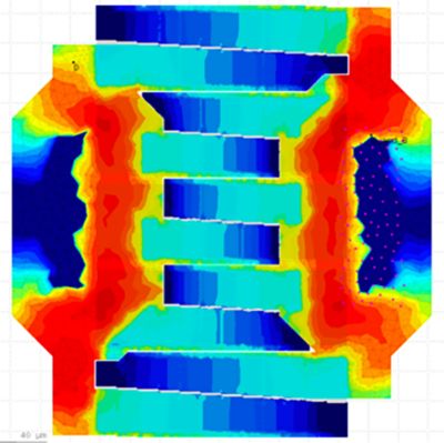
A power MOSFET layout with colors overlaid to show current densities throughout the device and current crowding at sharp corners. The top left corner has the colors removed to show the underlying 2D mesh created by the Ansys PowerX tool for this analysis.
Simulating with Ansys PowerX Software
To address the unique requirements of power device analysis, the Ansys PowerX tool for power field-effect transistor (FET) and PMIC analysis, simulation, and optimization was created as a purpose-built power transistor simulator. The PowerX tool is an extension of the widely popular Ansys ParagonX integrated circuit design analysis and parasitic debugging tool. It offers the same ease of use as ParagonX software and the same fast and easy setup. Many power MOSFET designers do not have the luxury of large support teams to develop and maintain semiconductor tool flows. The PowerX application eliminates this issue by making it very simple for any design team member to set up their own simulations using information that is readily available to them, with very little training needed. Necessary information such as layer resistivities, RDSon, and port locations can be easily defined by the user directly in the graphical user interface (GUI), and novice users can start running simulations very quickly with reasonable default settings. The PowerX tool can also read a foundry physical design kit (PDK) if one is available.
The power device itself is just one piece of a complex system. Design engineers want to simulate how the power device works in context of a larger system, including a package and PCB. Simulating the device without including those elements can miss their large effect on current distribution. The PowerX tool enables engineers to easily add those layers with the click of a button.
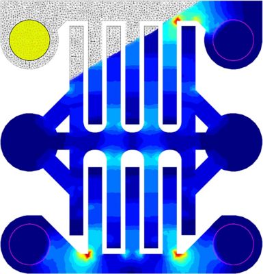
An analysis of current density without the addition of a PCB.
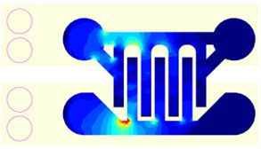
An analysis of current density with the addition of a PCB. The PCB addition changes the analysis results significantly and is important for simulating the device in full to achieve reliably accurate results.
Enabling Confident, End-to-End Power Design
Comprehensive graphical visualization of the simulation results enables designers to easily debug issues and find bottlenecks and weak points in the device. Identifying the layers that contribute the most to total resistance saves a lot of time. The PowerX tool makes it easy to visualize electromigration and current uniformity across bumps, balls, and bondwires. For instance, some tools provide a comprehensive list of every single resistor that violates electromigration limits, which can amount to thousands. This can be overwhelming and not particularly useful. PowerX software organizes these violations, so designers only need to examine a few dozen violations instead of thousands. It enables designers to make informed decisions by addressing questions such as, “Do I have enough bumps?” and “Are all of my ports being utilized efficiently?”
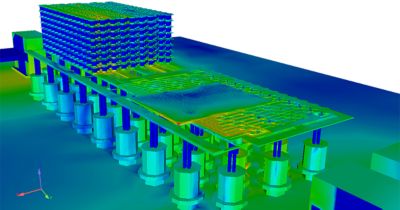
Another strength of the PowerX tool is its ability to deal with complex curvilinear shapes and angular polygons. Other tools struggle to describe these shapes, which can lead to false or missed areas of high current density. The PowerX tool has a unique finite element mesh that represents a much more physical and accurate picture of current density, giving users the confidence that what they send to the silicon foundry will be of the highest quality.
The PowerX tool offers a unique option to perform electrical analysis early in the design process before a layout is complete. This rapid analysis enables the layout engineer to quickly iterate over different geometry options. Without early analysis, engineers may spend days or weeks creating a completed layout, only to discover during simulation that the top layers are not optimal, resistance is too high, or current density hotspots exist — which may require a complete redesign. The ability to quickly create rough polygons and simulate current density and resistance gives a high degree of freedom to design teams, marking a major step forward in layout optimization. It opens the possibility of real innovation in power MOSFET design.
A sophisticated PowerX analysis uses color coding to show how sensitive the device resistance is to contributions from different areas of the MOSFET. This enables the designer to quickly identify which sections need careful optimization to avoid misdirected effort and time savings.
The PowerX tool makes power device simulation approachable by following the successful ParagonX methodology: simple, clear inputs; detailed results tables; and powerful, intuitive visualization. It provides all the essential features a design team needs to ensure the quality, robustness, and reliability of power devices and PMICs. Additionally, the software supports several data formats for final verification, including GDS, CCI, and PVS files.
As devices get smaller, faster, and more power-hungry, designing efficient and reliable power systems becomes even more critical. Ansys simulation gives engineers a way to test their ideas early, catch issues faster, and explore bold new designs with confidence. As technology pushes boundaries, simulation rises to meet this challenge with precision, speed, and accessibility, enabling us to keep the lights on, the batteries full, and innovation moving forward.
Learn more about the Ansys PowerX tool and other Ansys semiconductor solutions here. Download the Optimizing Analog Design with Multiphysics e-book here.
Just for you. We have some additional resources you may enjoy.


The Advantage Blog
The Ansys Advantage blog, featuring contributions from Ansys and other technology experts, keeps you updated on how Ansys simulation is powering innovation that drives human advancement.