-
-
Access Free Student Software
Ansys empowers the next generation of engineers
Students get free access to world-class simulation software.
-
Connect with Ansys Now!
Design your future
Connect with Ansys to explore how simulation can power your next breakthrough.
Countries & Regions
Free Trials
Products & Services
Learn
About
Back
Products & Services
Back
Learn
Ansys empowers the next generation of engineers
Students get free access to world-class simulation software.
Back
About
Design your future
Connect with Ansys to explore how simulation can power your next breakthrough.
Free Trials
ANSYS BLOG
March 28, 2024
Spark Photonics and Ansys Shape Leaders and Learners in Photonics Tech
If you're looking to start your education or career in a booming field, integrated photonics might be the right path for you. It's a field defined by strong growth: recent projections indicate that the global photonic integrated circuit (PIC) market will reach $30.4 billion by 2028, with an anticipated compound annual growth rate of 19.6% between 2023 and 2028.
The field of photonics deals with the physical science and application of light particles (photons) that form the basis of many light-based applications including high-speed data communications, imaging, and advanced sensing. Integrated photonics, then, are photonics that have essentially been miniaturized and integrated onto the surface of a chip.
Electric field monitor
Integrated photonic devices’ dimensions are typically measured in microns, in which one micron is one-thousandth of a millimeter. To give you a bit more perspective, your fingernails grow 3 to 3.5 millimeters per month on average. So, it's technically possible to put thousands of photonic devices on the tip of your fingernail.
As you might expect, designing photonic devices that are not visible to the human eye is inherently complex. This is where both a high level of specialization and simulation come into play.
Breaking It Down to Microns with Simulation
So, how do you successfully design at the micron scale to deliver photonic devices? Spark Photonics has the answer. The company is a one-stop shop for scalable photonics design enabled by its in-house design expertise and photonic integrated circuit (PIC) design software. They rely on the support of the Ansys Startup Program and Ansys simulation software — not only to optimize their designs, but also as the basis for training skilled professionals to support future innovations.
"We do end-to-end PIC design and layout for our customers, starting with the most fundamental components, which is really where Ansys comes in," says Kevin McComber, CEO of Spark Photonics. "We depend on simulation for iterating and coming up with novel components, then taking those components all the way to the layout stage, where the circuit is reduced to a blueprint that is sent to the foundry for fabrication. Ansys Lumerical works seamlessly with our layout software as well, so it’s a great end-to-end design flow."
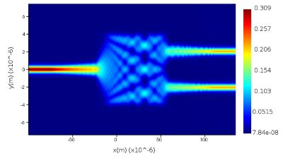
1x2 multi-mode interference (MMI) simulation in Ansys Lumerical EME. The EME method is used for modelling guided optical components (wave guides).

Final multi-mode interference design
According to McComber, there's a real push to expand integrated photonics into other areas and develop new applications around it, which is good for business. Yet the inherent level of complexity involved in producing anything at the micron level makes growth a challenge without the right software.
"We're creating potentially thousands of components in a form factor that we are unable to validate with our eyes," says Cooper Hurley, photonics design engineer at Spark Photonics. "And these components we're designing, in addition to having certain tasks they are supposed to perform, have to work across different wavelengths of light. Simulation helps us visualize and create these structures, then create signals inside the software to simulate device performance on a component scale."
Spark Photonics' work is very exacting, involving numerous Ansys tools and solvers to speed through design iterations. From there, the team takes the resulting components working at very specific wavelengths or frequencies of light and adapts them to specific situations to fit customer needs. While it seems like the process of transferring components working at one frequency to work at another should be a slam dunk, it's an iterative optimization process involving a lot of design considerations.
Without simulation — and support from the Ansys Startup Program — all this testing and iterating with physical prototypes would be too costly. The program offers simulation software custom-bundled at affordable pricing, which gives early to mid-stage startups like Spark Photonics access to the tools and solvers needed to solve complex engineering challenges.
Spark Photonics' workflow, for example, is heavily tied to Ansys Lumerical Multiphysics photonics component simulation software. Access to Lumerical Multiphysics enables the team to quickly go through as many iterations on a computer as they need to optimize their designs before settling on a final one.
Physical prototyping of PIC designs, on the other hand, is expensive. Some chips, depending on the application, can cost thousands of dollars per chip to build. Lumerical Multiphysics enables the team to optimize and then test their designs virtually to significantly reduce the number of physical prototypes needed for final verification and validation.
2D simulation of a grating coupler in Ansys Lumerical FDTD. Grating couplers are commonly used optical interfaces in integrated photonics for coupling light.
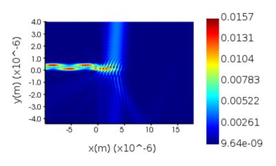
Power monitor of the 2D grating coupler simulation in Ansys Lumerical FDTD.
Taking AIM at First-Time Photonics Development Success
Another aspect to Spark Photonics' service model is its process design kit (PDK) development services. A PDK is an entire suite of documentation and technology files that enable designers to design into a foundry. Essentially, PDKs enable designers to use a given foundry technology.
Within a given PDK, there are numerous items. There's documentation of the technology including design rules that a user must obey, as well as software files that allow design tools to work with the PDK. There's also a library of pre-designed, pre-validated components that in many cases have already been fabricated and tested for certain applications.
With access to this library, it's then possible to adapt these existing components around an established group of rules into a circuit — instead of having to design everything from scratch.
Since 2020, Spark Photonics has been developing PDK libraries for AIM Photonics, an integrated photonics foundry based in upstate New York. AIM Photonics recently announced the release of the second Spark Photonics library, this time on AIM’s silicon nitride platform, that enables designers to access wavelengths in the 700-1300 nanometer range for applications as diverse as chemical sensing, atomic clocks, and quantum computing.
Of course, the strategy here is to help Spark Photonics’ and AIM Photonics’ customers save both time and money while driving first-time success in photonics device development.
Grating coupler simulation
"Spark’s AIM Photonics component library was largely developed and continues to be developed using Ansys software," says McComber. "Within the library we've included important devices like splitters, couplers, and waveguides. Users can take those components that have already been designed, and in a lot of cases already fabricated and tested, and incorporate them into a larger design. So instead of trying to design everything themselves, they can just hook the components together using waveguides, see how the circuit works, and proceed to layout and fabrication."
Simulation Nurtures Sparks of Genius
Forging a relationship with Ansys helped McComber solve complex design challenges without breaking the budget. But can it help him build a workforce of qualified technical professionals specifically trained in photonics? Education and simulation are key to this effort.
It was a pressing need for industry talent that inspired McComber to start a separate company, the Spark Photonics Foundation. With funding from the U.S. government, the 501(c)(3) nonprofit teaches K-12 and college students about concepts in STEM and advanced manufacturing using semiconductors and photonics technology through a project-based learning program called SparkAlpha. With support from Ansys, Spark Photonics has facilitated this program to reach more than 500 students across Massachusetts.
"The foundation has received funding from Ansys as a corporate donation to expand the SparkAlpha program that will be used in part to train teachers to run our program," adds McComber.
The SparkAlpha program exposes students to applications of integrated photonics, including chemical sensing and machine vision. It also includes in-person and virtual trips to local colleges and companies working in the semiconductor supply chain. At the end, there is a "Shark Tank”-like student competition, in which students share and are evaluated on their best ideas. Additionally, the foundation is launching SparkBeta, a program that teaches students Python coding and how to use it to design photonic chips.
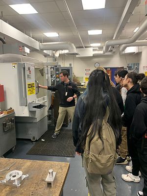
SparkAlpha students touring Governors America Corporation (Agawam MA) for Industry Day.

SparkAlpha students collaborating on conceptualizing their device using photonic sensors.
Ansys Helps Inspire a New Generation of Photonics Experts
So where does simulation fit into the work of the foundation? By introducing Ansys simulation into the classroom in the near future, SparkAlpha and SparkBeta hope to provide students with additional insights and skills they can leverage on the job.
"One of the lessons we learned from discussions with potential partner schools is the continued misunderstanding of what manufacturing jobs are these days," says Robert Vigneau, director of educational outreach programs at the Spark Photonics Foundation. "I think simulation broadens a student's concept of what manufacturing is. Using Ansys simulation, they get an entirely new perspective. In a simulation environment, they can model and test a product virtually, highlighting the process of producing a product in advanced manufacturing facilities."