-
-
학생용 무료 소프트웨어에 액세스하기
차세대 엔지니어에게 힘을 실어주는 Ansys
학생들은 세계적 수준의 시뮬레이션 소프트웨어를 무료로 이용할 수 있습니다.
-
지금 바로 Ansys에 연결하십시오!
미래를 설계하기
시뮬레이션이 다음 혁신을 어떻게 지원할 수 있는지 알아보려면 Ansys와 연결하십시오.
국가
무료 트라이얼
제품 및 서비스
학습하기
회사 정보
Back
제품 및 서비스
주제 상세 정보
ASIC 설계 흐름: ASIC 설계란?
ASIC란?
ASIC는 응용 분야별 집적 회로의 약어로, 전자 시스템 내에서 특정 기능 또는 일련의 기능을 수행하도록 정밀하게 설계된 특수 유형의 집적 회로입니다. 전자레인지 또는 TV 박스와 같은 일상적인 전자 장치의 범용 마이크로프로세서와 달리 ASIC은 특정 응용 분야에 맞게 맞춤형으로 제작되어 탁월한 효율성과 성능을 제공합니다.
ASIC는 다양한 전자 제품을 포함하여 외부 전자 회로 요구 사항을 최소화합니다. 특정 응용 분야에 맞게 맞춤 제작되는 특성으로 인해 ASIC 개발에는 더 높은 비용이 발생할 수 있습니다. 그러나 이 비용은 합리적이며 대량으로 제품을 만들 때 좋은 투자로 간주될 수 있습니다.
ASIC 설계의 유형
ASIC 설계에는 두 가지 기본 방법이 있습니다.
- 게이트 어레이(반맞춤형 설계)
- 완전 맞춤형 설계
반맞춤형 설계는 몇 개의 그룹으로 나뉩니다. ASIC의 분류는 다음과 같습니다.
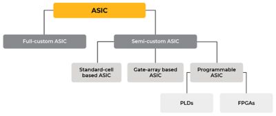
ASIC의 유형
경우에 따라 프로그래밍 가능한 ASIC는 반맞춤형 ASIC와 별개로 간주됩니다. 기타 ASIC 분류는 다음과 같습니다.
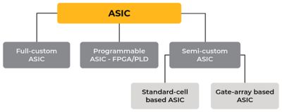
ASIC 분류
완전 맞춤형 설계: 완전 맞춤형 방식은 더 복잡하고 비용이 많이 들지만 게이트 어레이 방식보다 훨씬 많은 작업을 수행할 수 있습니다. 설계에 필요한 게이트 및 전자 장치만 통합되고 사용되지 않는 게이트가 삭제됨에 따라 ASIC의 크기가 크게 줄어듭니다. 이러한 ASIC는 특정 목적을 위해 설계되었으며 최종 제품의 특정 기능을 지원합니다.
반맞춤형 ASIC: 이 접근 방식은 확산된 레이어, 트랜지스터 및 기타 활성 장치를 사전 정의하여 초기 설계 노력을 최소화함으로써, 반복되지 않는 엔지니어링 비용을 절감합니다. 완전 맞춤형 설계에 비해 상대적으로 빠른 공정인 금속화 공정을 활용하기 때문에 생산 주기가 크게 단축됩니다. 최종 설계 단계에서 엔지니어는 특정 스위치를 조작하여 원하는 사양에 따라 칩의 동작을 안내합니다.
표준 셀 기반 ASIC: 이 유형의 ASIC는 게이트, 멀티플렉서 및 플립플롭과 같은 표준 셀이라고 불리는 미리 설계된 논리 셀을 사용합니다. 표준 셀은 완전 맞춤형 설계 방법을 사용하여 만들어졌으며 ASIC 설계를 위한 기본 구성 요소 역할을 하여 동일한 성능과 유연성을 보장하지만 시간과 위험을 줄입니다.
게이트 어레이 기반 ASIC: 이 범주의 ASIC에서는 트랜지스터, 로직 게이트 및 기타 능동 소자가 실리콘 웨이퍼 상에 생성되고 제조되는 반면, 제조 중에는 상호 연결이 형성되지 않습니다. 게이트 어레이 상에 미리 설정된 트랜지스터들의 배열을 베이스 어레이(base array)라 하고, 게이트 어레이를 구성하는 가장 작은 반복 요소를 베이스 셀(base cell)이라 합니다. 이 접근 방식에는 짧은 처리 시간, 더 높은 논리 밀도 및 접촉 계층 사용자 지정 등 여러 가지 이점이 수반됩니다.
프로그래밍 가능한 ASIC: 이러한 유형의 ASIC는 제조 후 하드웨어 수준에서 프로그래밍할 수 있습니다. 특정 응용 분야에 맞게 맞춤 설계 및 제작된 기존 ASIC와는 달리, 프로그래밍 가능한 ASIC는 일정 수준의 유연성과 재프로그래밍을 제공합니다. 프로그래밍 가능한 ASIC의 완벽한 예로는 프로그래밍 가능 논리 장치(PLD)와 현장 프로그래밍 가능 게이트 어레이(FPGA)가 있습니다.
ASIC의 응용 분야
ASIC은 다양한 산업 분야에서 각각 고유한 목적을 위해 기술을 활용하는 응용 분야를 찾습니다. ASIC가 중추적인 역할을 하는 주요 분야는 다음과 같습니다.
가전제품: ASIC는 가전제품, 스마트폰, 디지털 카메라, 스마트 TV 등의 전원 장치에 어디에나 존재합니다. 맞춤형 솔루션을 제공하는 능력은 이러한 장치의 전반적인 성능과 전력 효율성을 향상시킵니다.
통신: ASIC는 네트워킹 장비, 라우터 및 통신 장치에 사용됩니다. 맞춤형으로 설계된 특성으로 인해 데이터 처리 시 최적의 기능과 속도가 보장됩니다.
자동차 산업: ASIC는 엔진 제어 장치(ECU), 첨단 운전자 지원 시스템(ADAS), 인포테인먼트 시스템과 같은 다양한 시스템에 통합되어 자동차 산업에 크게 기여합니다.
헬스케어: 의료 장비, 진단 장비 및 이미징 시스템에는 정밀도, 신뢰성 및 전력 효율성에 대한 엄격한 요구 사항을 충족하기 위해 ASIC가 통합되는 경우가 많습니다.
ASIC 설계 프로세스
ASIC 설계는 고도로 전문화된 칩을 만드는 데 기여하는 여러 단계를 포함하는 정밀한 프로세스입니다. ASIC 설계의 주요 단계는 다음과 같습니다.
사양 및 요구 사항: 이는 설계 프로세스를 시작하기 위한 사양과 요구 사항을 정의하는 ASIC 설계 흐름의 첫 번째 단계입니다. 관련 이해관계자의 의견을 수집하고 전체 제품 사양을 상세한 기술 사양으로 변환하는 작업으로 구성됩니다. 예상 출력, 성능 목표, 전력 소비 목표 및 기타 필수 매개변수를 명확하게 설명해야 합니다.
아키텍처 설계: 사양이 마련되면 ASIC의 아키텍처가 설계됩니다. 여기에는 전체 구조, 기능 블록의 배열 및 이러한 블록 간의 상호 연결을 결정하는 작업이 포함됩니다. 엔지니어는 할당된 예산 내에서 전체 비용을 유지하면서 성능 영향, 기술적 타당성 및 하드웨어 리소스를 신중하게 고려하여 가능한 많은 아이디어를 브레인스토밍하고 이상적인 접근 방식을 선택해야 합니다.
RTL 설계: RTL(레지스터 전송 수준) 설계에는 HDL(하드웨어 설명 언어)을 사용하여 ASIC의 기능을 설명하는 작업이 포함됩니다. 이 단계는 추상적인 아키텍처 설계와 물리적 구현 사이의 가교 역할을 합니다.
검증: 검증은 테스트 벤치에서 설계를 테스트하고 시뮬레이션하여 ASIC가 지정된 요구 사항을 충족하는지 확인합니다. 이 단계는 설계 결함이나 문제를 식별하고 수정하는 데 중요합니다.
합성 및 구현: 합성 중에 RTL 코드는 게이트 레벨 넷리스트로 변환되어 ASIC의 물리적 구현을 나타냅니다. 이 넷리스트는 레이아웃으로 변환되며 물리적 설계는 전력 소비, 속도 및 영역에 최적화됩니다.
사인오프 및 테이프아웃: 물리적 레이아웃을 완료한 후 다음 단계는 파운드리에서 권장하는 설계 규칙에 따라 물리적 설계를 확인하는 것입니다. 엔지니어는 LVS(Layout-versus-schematic) 검사 및 설계 규칙 검사를 수행하며, 이 검사는 시뮬레이션 도구를 사용하여 필요한 곳에서 설계를 수정합니다. 이 프로세스를 사인오프라고 합니다. 설계가 지정된 설계 규칙을 통과하면 테이프로 아웃하여 파운드리로 보내져 제조됩니다.
제조: 마지막 단계는 반도체 제조 공정을 사용하여 ASIC를 제조하는 것입니다. 이 단계에서는 맞춤형으로 설계된 칩을 생산할 수 있는 반도체 파운드리와의 협업이 필요합니다. 제대로 된 파운드리를 선택하면 원하는 결과를 얻는 데 도움이 됩니다.
ASIC의 장점
성능 최적화: ASIC은 특정 작업에 탁월하도록 설계되었으며 전용 기능을 위한 필수 회로만 갖추고 있습니다. 간소화된 설계는 크기와 전력 소비를 줄여 범용 프로세서를 능가하는 탁월한 성능과 효율성을 제공합니다.
전력 효율성: ASIC의 맞춤형 특성으로 인해 불필요한 구성 요소를 제거하여 전력 효율성을 향상시키고 에너지 소비를 줄일 수 있습니다.
공간 최적화: ASIC은 특정 폼 팩터에 맞게 맞춤화할 수 있으므로 전자 장치의 공간 효율적인 설계가 가능합니다.
대량 생산 시 비용 효율적: ASIC 설계 및 제조의 초기 비용은 상당할 수 있지만, 중복 구성 요소가 없기 때문에 대량으로 생산할 경우 비용 효율이 높아집니다.
성능 및 효율성 향상은 전자 산업에서 항상 최우선 순위 목표입니다. ASIC의 응용 분야별 특성이 업계 전반에 미치는 영향은 명백하며 혁신을 촉진하고 전자 장치의 기능을 향상시킵니다. ASIC의 설계 프로세스를 보다 효율적이고 신속하며 비용 효율적으로 만들려면 설계 및 시뮬레이션 소프트웨어를 신중하게 선택해야 합니다. 속도가 빨라지고 크기가 작아짐에 따라 설계자는 기존 기술을 뛰어넘어 새로운 다중물리 문제를 해결해야 합니다.
여기에서 다중물리 시뮬레이션의 중요성에 대해 자세히 알아보십시오. Ansys 반도체 솔루션
관련 리소스
시작하기
엔지니어링 과제에 직면하고 있다면우리 팀이 도와드리겠습니다. 풍부한 경험과 혁신에 대한 헌신을 가지고 있는 우리에게 연락해 주십시오. 협력을 통해 엔지니어링 문제를 성장과 성공의 기회로 바꾸십시오. 지금 문의하기