-
-
학생용 무료 소프트웨어에 액세스하기
차세대 엔지니어에게 힘을 실어주는 Ansys
학생들은 세계적 수준의 시뮬레이션 소프트웨어를 무료로 이용할 수 있습니다.
-
지금 바로 Ansys에 연결하십시오!
미래를 설계하기
시뮬레이션이 다음 혁신을 어떻게 지원할 수 있는지 알아보려면 Ansys와 연결하십시오.
국가
무료 트라이얼
제품 및 서비스
학습하기
회사 정보
Back
제품 및 서비스
ANSYS ADVANTAGE MAGAZINE
DATE: 2020
Blueprint for Success
Ansys Dimensions Staff
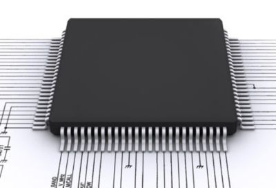
Tiny yet powerful, semiconductor chips support the success of every futuristic technology you can imagine — from driverless cars and self-guided rockets to 5G-enabled devices and cryptocurrency. Designing these chips with customized functionality for each application is a challenging task, complicated by the need to fit into ever-smaller packages. That is where INVECAS comes in. Only four years old, this India-based startup is a global leader in designing advanced IP and ASICs. Recently, VP of Engineering Srinivasa Gutta spoke with Dimensions about the company’s challenges and opportunities.

DIMENSIONS: What are the biggest trends today in semiconductor engineering — and how are they impacting INVECAS?
SRINIVASA GUTTA: Certainly the biggest trend is the need to develop more innovative, more customized semiconductor chips that support very specific customer needs. These are called application-specific integrated circuits (ASICs), and demand is growing rapidly as everyday products become smarter and more complex.
If you think about the modern car, there are many technology systems that must work seamlessly together — from mission-critical functions like braking and airbag deployment to entertainment, navigation and comfort systems. Autonomous driving only adds to this complexity. All this diverse functionality — which includes sensing, signaling and communications — is delivered by semiconductor chips. Each chip has to perform optimally on its own and also as part of a larger system.
INVECAS was founded in 2014 by a team of semiconductor experts to serve this market need. We develop a range of intellectual property (IP), including highly specific, extremely customized chip designs that provide targeted functionality. We partner with silicon manufacturing foundries that bring our designs to life. These close relationships ensure that our IP functions ideally not only in isolation, but as part of a larger system.
A related trend is the demand for an accelerated design cycle. If we go back to the autonomous vehicle example, every automaker is in a race to launch new self-driving cars ahead of the competition. This places incredible pressure on INVECAS to come up with standard IP and new chip blueprints very quickly. At the same time, our IP has to go through rigorous testing and certification to meet uncompromising standards and requirements.
Before we invest in costly prototype fabrication and testing, simulation provides us with a very high degree of certainty that our IP and chip designs will perform as anticipated.
AD: How does INVECAS balance design speed with the mission-critical nature of your product applications?
SG: From our company’s inception, we have relied on engineering simulation to verify the performance of our IP designs at a very early stage. We’ve invested $5 million in a 5,000-square-foot physical testing facility, but we need to leverage that resource strategically. Before we invest in costly prototype fabrication and testing, simulation provides us with a very high degree of certainty that our IP and chip designs will perform as anticipated.
Simulation via Ansys helps us balance an accurate logical design — which delivers the desired functionality — with an optimal physical design in terms of size, thermal footprint and other characteristics. Our engineers can make intelligent trade-offs that optimize power, performance and area, which are our three most important metrics. Our designs are produced in a continuous loop, beginning with the customer’s specification — for example, the IP must operate at a 3.6 GHz frequency, or transmit data at 16 gigabytes per second. We simulate these operating parameters, track key performance metrics and conduct iterative simulations that optimize the IP design.
What’s unusual about the semiconductor business is that the closed-loop simulation process does not end when we hand off the schematic or graphic data system (GDS) to manufacturing. INVECAS fabrication partners also use a common simulation platform, Ansys Redhawk, which allows us to easily pass designs and prototypes back and forth.
This seamless design, simulation and fabrication process gives our customers extreme confidence in our intellectual property — and accelerates the design-and-fabricate cycle. The idea of simulating the manufacturing process is gaining ground in other industries, but it has always been foundational to the semiconductor industry. It ensures that performance is verified at every stage.
AD: In just four years, INVECAS has grown to 1,300 employees worldwide. What is the secret to your success?
SG: Engineering excellence is critical, because we are creating intellectual property which has to be better than the solutions of our competitors. Ninety-five percent of our employees are engineers. We have worked hard to hire the right talent and create a collaborative, energized team that is excited about creating cutting-edge designs. From its inception, INVECAS has been focused on building the right company infrastructure, attracting the best people and providing them with best-in-class technology tools.
Our collaboration with Ansys is a great example. From the beginning, we identified Ansys Redhawk as the best simulation platform for the kinds of complex modeling we need to accomplish. Today, 50 percent of our analog engineers use Ansys software to perform challenging tasks like power modeling, and designing for analog and mixed-signal environments. These are not simple simulations, and we’ve been consistently impressed by the software’s capabilities and accuracy. Ansys simulations form the basis for every one of our designs.
Beyond the quality of the software, what has been important to INVECAS as a startup is that Ansys has functioned as a true partner, not just a software vendor. The Ansys team has helped train our people, define new workflows, create new power models and anticipate our evolving simulation needs. Ansys is invested in our success, and we have felt that from the beginning.
Everyone is betting on 5G to emerge as the backbone of communications in the near future.
AD: Looking into the future, what lies ahead for the semiconductor industry — and how is INVECAS preparing for that future?
SG: Everyone is betting on 5G to emerge as the backbone of communications in the near future. While household names like Apple and Samsung will drive this transformation, the effects will impact everyone in the electronics industry, including semiconductor designers and fabricators. INVECAS will need to design new ASICs and other intellectual property that meet an entirely new set of operating parameters to support 5G.
The continuing electrification and autonomy of cars is another trend we are watching very closely. As cars become more like data centers — constantly gathering, analyzing and responding to information — we need to design our chips differently. They not only need more capabilities in smaller and smaller packages, they also need to perform reliably in harsh, unpredictable environments. Cars also have a relatively long product life, so we need to account for the aging of our chip designs. We are using simulation right now to replicate the effects of aging, and we need to increase that effort. Eventually we might begin to explore the use of digital twins to capture real-world data and understand the aging process in real time.
Finally, machine learning and artificial intelligence are exciting trends that we are watching. As products become smarter and able to gain knowledge, there’s no telling what impact that can have on the world as we know it. At INVECAS, we are looking at the enabling semiconductor technologies and the next-generation IP that will create the foundation for artificial intelligence. None of us are sure what this “brave new world” will look like, but one thing is certain: Chip designs will have a foundational role in making it possible.