Synopsys and Ansys power the future of innovation—connecting silicon to systems.
-
-
학생용 무료 소프트웨어에 액세스하기
차세대 엔지니어에게 힘을 실어주는 Ansys
학생들은 세계적 수준의 시뮬레이션 소프트웨어를 무료로 이용할 수 있습니다.
-
지금 바로 Ansys에 연결하십시오!
미래를 설계하기
시뮬레이션이 다음 혁신을 어떻게 지원할 수 있는지 알아보려면 Ansys와 연결하십시오.
무료 트라이얼
제품 및 서비스
학습하기
회사 정보
Back
제품 및 서비스
ANSYS BLOG
December 4, 2020
No Limits: Ansys HFSS 3D Layout for Every Engineer
To push the envelope of electronic innovation, engineers must integrate more functionality with reduced power consumption into smaller footprints. And to win the race to market, engineers must confidently simulate the resulting complex design faster than ever before.
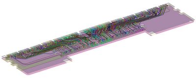
DIMM design courtesy of Smart Modular Tech, smartm.com
Today’s engineering managers need their teams to simulate and iterate designs quickly with minimal expensive engineering set up time. This may pose a challenge if they have neither the time nor the resources to find and recruit engineers with deep simulation expertise. Instead, they need engineers armed with the right product and design skills — who are not necessarily experts in computational electromagnetics — and give them access to Ansys HFSS. For layout-based designs (e.g. PCB, IC package, interposer, or IC), it is critical from a workload efficiency standpoint to leverage the right simulation flow, Ansys HFSS 3D Layout.
Historically, many HFSS users designing in layout could not imagine simulating a complex design such as an entire DIMM module because working in the classic HFSS 3D workflow could require days to set up and solve. Consequently, engineers resorted to breaking up large designs and simulating smaller, partial designs. This approach can compromise the accuracy of the analysis.
For these types of designs HFSS 3D Layout can reduce model set up time from hours to minutes with a flow mapped directly to the design tool. Leveraging knowledge about the geometry such as stackup, power, ground and pin locations, and working with geometry primitives such as traces, vias and pads, HFSS 3D Layout can automate much of the setup effort. By transferring the time-consuming burden of set up from human to machine and leveraging HFSS’s elastic hardware capability, HFSS 3D Layout can solve larger and more complex models than thought possible before.
In the end, development costs are slashed with this optimized simulation workflow, significantly advancing the innovation of next-generation products.
Speeding Simulations of Complex Designs
HFSS 3D Layout was recently put to the test by simulating a highly complex SO-DIMM module, composed of an eight-layer PCB with eight, two-layer modules, 64 nets and 128 ports. Using HFSS 3D Layout, set up time was a matter of minutes and with Ansys HFSS’s latest HPC solver, technology results were turned around quickly for a very complex design.
Design set up was incredibly simple. After importing the design files, an automated workflow arranges and aligns the assembly. Then, an integrated Pin to Pin utility identifies the components and their pins and automatically sets up the excitations to generate the s-parameter model for the assembly. Pin to Pin can also cut out a sub-design from the larger layout for more focused simulations. Next, using an auto solution set up, the engineer defines the desired frequency sweep, selects a trade-off of accuracy versus speed and the simulation is ready to go.
To run the solution, HFSS is enabled on Ansys Cloud, built on Microsoft Azure. Solver access to Ansys Cloud is via an intuitive, integrated portal. The user chooses a machine configuration, and the simulation is off and running. For post-process, results can either be downloaded from within the portal or accessed remotely in a virtual desktop infrastructure (VDI) browser session within Ansys Cloud, eliminating the need to download solution data.
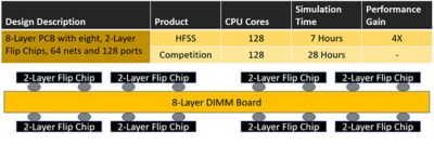
Recently, HFSS 3D Layout and Ansys Cloud joined forces to solve this SO-DIMM. Using a four-node, 32 cores per node Ansys Cloud configuration, the entire simulation process consumed only seven hours. This included 45 minutes of initial meshing, two and a half hours of adaptive meshing, and three hours and forty-five minutes for the frequency sweep. The speed was delivered without compromise to the design or to accuracy.
Under the hood, Ansys HFSS’ meshing and hardware elastic distributed memory matrix (DMM) solver powered this fast Ansys Cloud simulation. By using DMM, a fully coupled electromagnetic matrix was solved to ensure that no interactions were missed or swept under the rug. No behind the scenes auto-simplification was performed, such as removing real voids in the power/ground structure. Additionally, there was no need to resort to a “divide and conquer” approach, using stitched together s-parameter models. Because the simulation runs in just a handful of hours, an engineer can quickly iterate through multiple variations to achieve an optimal design.
Speeding Simulations of Complex Designs
With continued research and additional development breakthroughs, HFSS was able to solve this same model even faster. In fact, HFSS cut simulation time by more than 20%, from seven to five and a half hours, while covering a bandwidth from DC to 50 GHz. And there’s more to come! Look for a huge HFSS technology breakthrough arriving in Ansys 2021 R1 early next year.
At this frenetic pace, it is incredible to think how HFSS’s capacity and speed will improve to handle tomorrow’s even more challenging product designs. With this proven, powerful and cutting-edge technology, the sky is the limit.
Take a deeper dive into Ansys HFSS. Be sure to check out the many HFSS articles, white papers and webinars.