-
-
학생용 무료 소프트웨어에 액세스하기
차세대 엔지니어에게 힘을 실어주는 Ansys
학생들은 세계적 수준의 시뮬레이션 소프트웨어를 무료로 이용할 수 있습니다.
-
지금 바로 Ansys에 연결하십시오!
미래를 설계하기
시뮬레이션이 다음 혁신을 어떻게 지원할 수 있는지 알아보려면 Ansys와 연결하십시오.
무료 트라이얼
제품 및 서비스
학습하기
회사 정보
Back
제품 및 서비스
ANSYS BLOG
March 23, 2023
Using Underfill to Enhance Solder Joint Reliability
As more electronic assemblies are required to operate — and perform reliably for many years — in harsh environments, it becomes more critical to ensure that components can survive aggressive mechanical shock, drop, vibration, and temperature cycling events. One method to ensure that these components can operate reliably in these environments is adding the appropriate underfills and adhesives to printed circuit boards (PCBs).
What is Underfill?
Underfills are thermoset epoxies that are traditionally used in flip chip applications to reduce the thermal stresses on solder joints. The wide use of underfills started back in the late 1990s with Intel’s Pentium processor. Prior to the Pentium, most processors were wire-bonded silicon die on ceramic substrates. Intel recognized that by bonding the die directly to an organic substrate, performance could be increased and the cost reduced (Figure 1). However, due to the large coefficient of thermal expansion (CTE) mismatch between the die and the organic substrate, underfill was required to prevent the solder joints from failing during thermal cycling.
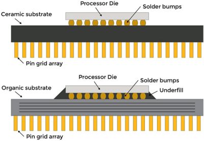
Figure 1: Ceramic and organic substrate CPU.
Today, underfills are not only used at the die (first level interconnect), but also to increase the reliability of ball grid array devices (second level interconnect) and are available in a variety of formulations. Underfilling ball grid array components reduces thermal and mechanical loads experienced by the solder joints. Careful consideration of the underfill material properties and the intended use environments must be made to assess the relative reliability improvements underfills offer.
Applications of Underfills
The image in Figure 2 is a contemporary flip chip package using a thick copper lid for heat sinking. Underfill is a critical component that protects the solder bumps from thermal stresses and package warpage during assembly and operation as well as against cracking of the die and in the low-k layers. Underfills act as a structural member between the die and substrate and provides load sharing that reduces the stresses solder joints are subjected to.
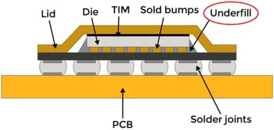
Figure 2: Flip chip underfill.
To reduce the thermal stresses on the solder bumps, a rigid underfill with a low coefficient of thermal expansion is required. Optimal selection of flip chip underfills CTE is in the range of 20 to 30 part per million per degree Celcius that are highly filled with silica particles and have a high glass transition temperature. The glass transition temperature (Tg) is the temperature at which the material properties of the material change. Most underfills are used below their Tg, which means that when the temperature goes above this, the material will soften and its CTE will increase.
Figure 3 shows a traditional over-molded flip chip package in which the board level solder joints are underfilled.
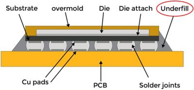
Figure 3: Board level underfill.
An important item to note is that BGA solder joints are much larger than the solder bumps for flip chip packages. The BGA solder interconnects can vary in height from 100 microns to 500 microns, which requires a much higher volume of underfill material when compared to a flip chip solder joint. The addition of underfill to the second level solder interconnects have shown to increase or decrease the fatigue life depending on the load environment and underfill properties. Reworkable underfills that show significant improvement under drop and shock loading but can degrade fatigue life under thermal cycling if thermal load environments exceed the underfills glass transition temperature. The CTE and modulus of underfills before and after the glass transition temperature will influence the fatigue of solder joints.
Materials
Conventional underfill materials are thermoset epoxies that contain silicon oxide particles, which provide stiffening. The particles reduce the coefficient of thermal expansion and increase the elastic modulus. Conventional underfill materials come in one- and two-part formulations, and deciding whether a one- or two-part is appropriate depends on:
- Curing temperature and time requirements
- Viscosity limitation (how well can underfills flow underneath a package?)
- Chemical resistance (would underfills be subjected to a corrosive environment?)
It is important to consider the different use cases for reworkable versus non-reworkable underfill materials. Reworkable underfill materials tend to not have any (or have very few) filler particles by volume. Non-reworkable underfill materials, on the other hand, offer high filler particles to reduce CTE and increase stiffness.
Methods
Underfills are designed to use the capillary action to flow underneath the part. Underfill is applied using a syringe, either manually or with an injecting device. One major benefit of the capillary method is that it enables manufacturers to customize inputs to ensure consistent flow and a fully covered package that is void-free.
A second underfill application process, which is becoming more popular, is the no flow underfill method. No flow underfill is designed to be cured during the solder reflow process — meaning the soldering and the underfill cure is done simultaneously. No flow underfills typically do not have filler particles to avoid constricting the soldering of the joints to the pads.
Simulation of Underfill
While underfilling is a decades-long technique, the materials implemented are continuously evolving in response to the growing needs of the electronics industry. New materials need to have their material properties fully characterized. To determine the fatigue performance can require extensive time and resources.
To learn more about how to use underfill to improve the reliability of your electronics, register for our upcoming webinar.