ANSYS 部落格
May 16, 2023
低功率 IC 設計:技巧與最佳實作範例
低功率 IC (積體電路) 設計是現代電子中的一大重要面向,因為其能延長電池續航力並降低裝置的耗電量。電池供電裝置的市場不斷成長,因此晶片設計師必須充分考量不同的技巧,以降低 IC 的耗電量。多項技術可用來降低 IC 的靜態與動態耗電量。DC 電流和漏電流是靜態功率的來源,至於動態功率則取決於頻率,端看電晶體切換和短路功率。
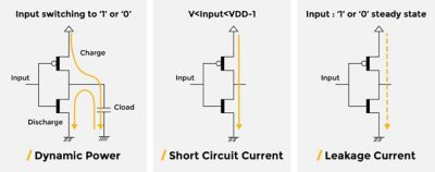
圖 1.互補式金屬氧化物半導體 (CMOS) 電路的功率元件
為了打造低功率的設計,Designer必須捨去會增加整體耗電量的所有個別功率元件。圖 1 顯示了動態和靜態功率特性。對互補式金屬氧化物半導體 (CMOS) 逆變器進行動態充電,會讓耗電量與時脈頻率成正比。無切換期間,透過電晶體產生的漏電則會造成靜態功率。
低功耗設計師可透過控制供應電壓、降低電路複雜度與時脈頻率,以及監控 DC 電流來源和切換節點的電容,進而降低總耗電量。一切都環環相扣,因此設計師必須進行測試並運用低功耗設計技術,取捨各項因素,藉此最佳化設計效能。
低功耗設計的技術與最佳實作範例
時脈閘控
降低裝置耗電量的其中一種方法是在暫存器傳輸級 (RTL) 調整設計。這是減少動態耗電量的最常見技術之一。在 RTL 層級,電晶體改變其邏輯狀態或使用電源為負載電容充電時,都會消耗功率。總動態功率為:
Pdynamic = Pcap + Ptransient = (CL + C) Vdd 2 f N3
其中 CL 為負載電容,C 是晶片的內部電容,f 是運作頻率,而 N 為切換的位元數。非必要時,對時脈進行閘控,即可輕鬆減少動態電流。相較於使用 AND/NOR 閘,較佳的方式是使用閂鎖型時脈閘控來避免任何額外耗電量。關閉傳送至 IC 特定部分的時脈訊號,可大幅降低耗電量,因為這些區域的電晶體就不會交換和消耗功率。
電源閘控
IC 中的所有區塊都不會持續運作;而這取決於其在裝置中的應用。如果某個區塊在特定情況下不會運作,則不需要為該區塊供電。透過關閉對未運作區塊的電源供應,即可降低耗電量。為了有效運用這項技術,設計師可使用隔離區塊,以防止來自電源閘控區塊的不必要訊號。
頻率閘控
如我們所知,晶片是由多個區塊組成,且每個區塊都不需要最高的可行運作頻率。最佳技術是根據區塊的頻率需求來分隔區塊,並針對不同區塊提供不同的時脈訊號。此方法可大幅降低 IC 的局部動態耗電量。
多電壓設計
在設計中,每個區塊運作的所需電量都不同。您可以根據區塊的效能及其電壓需求來分割晶片。電壓需求越高,耗電量就越高。建立具有不同電壓輸入的電壓島,可以輕鬆降低 IC 的整體耗電量。
動態電壓和頻率調整
前述電壓島技術有所限制,因為一旦供應至區塊的電壓供應設計完成,就無法於日後變更。動態電壓調整技術可讓設計師享有彈性,以根據需求於日後變更電壓。設計師可對調節器進行程式設定,以根據不斷變化的電流,變更對不同區塊的電源供應。同樣地,電壓調整也可以結合頻率調整,讓設計人員可在軟體程式的協助下,修改提供至每個區塊的時脈訊號。
降低功率
就降低功率而言,目前最重要的技術就是降低晶片的供應電壓。在 finFET 設計而中,動態切換功率佔有重要地位,且動態切換功率與供應電壓的平方成比例,因此出現推動採用超低電壓 (ULV) 製程的強勁趨勢。
漏電取捨
在前 finFET 技術中,漏電是一大功率耗用來源,最佳的控制方式則是透過多臨界電壓資料庫控制。這類資料庫可針對每個單元提供兩或三個版本,且各有不同的效能/漏電取捨。如此一來,設計師就能在時序關鍵路徑中使用快速的漏電單元,並在較不關鍵的路徑中使用較慢、低漏電的單元。
整體而言,有許多技術能幫助降低 IC 耗電量。透過這些技術,並使用適當的設計和模擬工具,設計師便能克服前述挑戰。Ansys RedHawk-SC 等工具,讓工程師可在每個設計階段模擬並預測設計行為,設計出更節能且電池續航力更持久的低功率 IC 產品。
低功率設計挑戰
- 壓降餘裕度變得非常吃緊,特別是在超低電壓設計中。這種演進讓電壓 (IR) 壓降簽核驗證成為所有現代 IC 設計中的重要環節。
- 供應電壓偏低會使路徑時序更容易受到動態壓降 (DVD) 影響。此外,分析 DVD 的涵蓋範圍是否足以擷取所有可能的切換情境,也極具挑戰。仔細的電壓降分析非常關鍵,如此才可將 DVD 對時序的影響降至最低,並避免因意外的 IR 壓降影響而造成頻率損失。
- 多電壓區域需要謹慎管理,方能確保不同電壓區域之間具有適當的訊號轉換和訊號完整性。UPF 是專為解決此挑戰而設計的標準。
- 再次開啟區塊時,電源閘控會帶來具挑戰性的轉換現象,且涵蓋電氣與邏輯層面。
- 在盡可能接近時脈分配網路根源的位置導入時脈閘控最為有效,但這受限於啟用訊號時序準時抵達的可行性。因此需要做出取捨,在實現電源效率與力求設計最佳化之間取得平衡。
任何功率分析的有效性均大幅取決於電路活動。然而,若要產生實際且具代表性的活動情境,以在所有模式中擷取實際使用方式的所有可能功率體制,並非易事。其中一種常見的錯誤是使用功能驗證活動向量來計算功率;這會造成誤導且與功率分析無關。良好的活動向量可以手動產生、透過功率工具 (「無向量」) 自動產生,或是透過執行實際應用的硬體模擬器產生。
Redhawk-SC 是軟體工具,廣泛用於 IC 設計中的功率分析。其提供全方位的功能組,以準確預測並分析晶片中的壓降,藉此解決前述問題。Redhawk-SC 使用複雜的演算法對晶片電力輸送網路的行為建模,並將晶片內電阻、電容和電感等因素納入考量。這讓 IC 設計師能夠識別潛在的壓降熱點,並在各種運作條件下模擬晶片的行為。設計低功率 IC 時,設計師必須考量電力輸送網路的所有層面,並在設計時預測電壓行為。
如需更多資訊,請造訪 Ansys RedHawk-SC 首頁,或是閱讀「Foundations of Semiconductor Power Integrity Analysis and Simulation(半導體電源完整性之分析和模擬的基礎)。」