產品系列
查看所有產品Ansys致力於為當今的學生打下成功的基礎,通過向學生提供免費的模擬工程軟體。
ANSYS BLOG
July 15, 2022
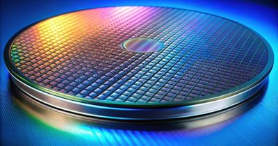
As semiconductor process technology development strives to squeeze out every last bit of achievable scaling from bulk silicon, it has pursued manufacturable silicon process nodes down to the stunning depth of 3 nanometers (nm). Achieving functionality in such geometries was thought impossible not long ago and is a tremendous engineering triumph. Nonetheless, the last decade of effort to further improve chip performance, density, and power has been a multidimensional engineering struggle, with node scaling complemented by hard-fought innovations in transistor design, silicon layering, tools and methodology development, and many other innovations.
A notable example of this is chiplet stacking in 3D integrated circuit (3DIC) packages, which from the beginning was an attempt to sidestep the derailment of Moore’s Law in ultra-deep submicron. 3DIC has unleashed an explosion of engineering creativity at the package and chip level, but it has also been accompanied by many unanticipated and very thorny problems.
One difficulty is the maintenance of clean, uninterrupted power distribution across chip die. Like its first cousin signal integrity (SI), power integrity (PI) has become a complex field that is vital to understand at the chip, package, and board level.
Even at just the chip level, the effects of proximity, materials, and design requirements for bandwidth and raw speed create a smorgasbord of power draw and electromagnetic interference (EMI) scenarios across frequencies ranging from MHz to GHz, along with physical scaling from micro to macro. But the chip level and all its complexities stemming from process features and circuit design represent only the first order of concerns in this complicated topic. There are dynamic signal and power interactions across the chip, package, and board level. Beyond that are further interplay issues going up to the system level, between systems themselves and even originating from more remote radio frequency (RF) sources.
Dr. Norman Chang and Dr. Altan Odabasi of Ansys have focused their decades of expertise on this set of PI challenges, leading the technical effort at Ansys to model and simulate PI in all its dimensions at the chip and package level. They have produced an on-demand webinar, “Foundations of Semiconductor Power Integrity Analysis and Simulation,” discussing the foundations of voltage (IR) and dynamic voltage drop (DVD) analysis and simulation for system on a chip (SoC) designs.
The webinar will examine multiple process technology features and their impact on power integrity in minute detail. RLC extraction and the development of IR/DVD modeling from a multiphysics perspective, including thermal, signaling, and RF effects, will be comprehensively examined. Finally, the numerical methods and operations for modeling and simulating these phenomena will be outlined and thoroughly explored.
Come join us for the seventh and final installment in our Electromagnetics Foundation webinar series. This concluding presentation promises to be one of the most in depth of a highly technical set of webinars.
我們將在此解答您的問題,並期待與您交流互動。Ansys 的銷售團隊成員會立即與您聯絡。