ANSYS BLOG
August 01, 2018
Artificial Intelligence Can Analyze Optical Material Properties from a Photo? Learn how!
Score one for our new robot overlords! Artificial intelligence (AI) can now read the optical material properties of a surface with a single click of your cellphone.

Digital reconstruction of surfaces (larger images) based on their photos (smaller images).
Researchers from Ansys’ optical simulation team (formerly OPTIS), Inria and MIT’s Computer Science and AI Lab have trained a computer to do what humans do instinctively: predict the feel of a surface by just looking at a photo.
In fact, this AI can deduce a material’s normal albedo, diffuse albedo, specular albedo and specular roughness for each pixel of an image. As a result, the tool could one day help engineers iterate their designs faster as they easily predict optical material properties.
“With a single picture, it is now possible to evaluate the behavior of light when it is in contact with materials,” explains Valentin Deschaintre, research engineer at Ansys. “A flashlight is used to lighten the object and a photo is taken. The AI then intuitively understands the material property based on the light’s behavior in the picture.”
How to Train AI to Predict Optical Material Properties
Humans are not great at programming a computer to recognize images. Therefore, the researchers had to teach the artificial intelligence to predict material properties from images where these values were known.
However, taking this AI to school was not easy. It required a data set of 200 000 procedurally generated spatially-varying bi-directional reflectance distribution functions (SVBRDF), 400,000 training iterations and a week or so of processing time on a TITAN X GPU.
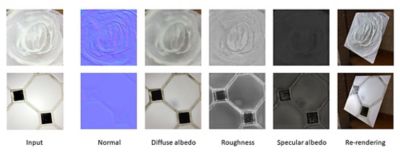
The AI uses the input photos (left images) to recover SVBRDF maps that describe the albedo and specular roughness (middle images). These maps are then used to re-render the image (right images).
“Artificial intelligence is a potent tool for this kind of issue as the computer can learn how to operate each visual index on the picture — such as shadows and reflections produced by the materials,” said Adrien Bousseau, head of research at Inria “Synthesis and image-based simulations are a critical element of this goal as we obtain the vast number of pictures that are required for this learning.”
Why Engineers Need Quick Optical Data
Engineers working with virtual prototypes, VR and simulations will find the tool useful to quickly determine a material property. This will allow them to focus on iterating their designs instead of finding ways to determine their optical data.
“Our research will be able to help engineers prototype their concepts quickly. This translates into an improvement in productivity,” noted Jacques Delacour, business director at Ansys.
Delacour isn’t kidding about that productivity boost. Typically, gathering this optical data would be done one small piece of material at a time. However, since this new tool can assess these properties on the level of a pixel, engineers can now assess a large surface at once.
“This data acquisition method has a big advantage when assessing large surfaces,” confirmed Deschaintre. “This new picture-based method allows you to learn about a broader surface, so you can capture big patterns quickly and easily.”
Future users of this material analysis method will also be able to save money as they reduce the amount of rigorous, yet expensive, lab measurements.
“An accurate lab measure of materials has been possible for several decades, but the required equipment is unreachable for many digital conception actors,” said Bousseau. “We aim to ease the acquisition of and objects’ appearance to be as simple as taking a picture with a cellphone.”
However, don’t cancel all lab measurements warns Delacour. He said, “Materials are complex —engineers need to study that complexity. As a result, materials will react differently to different light environments. To ensure accurate results and high quality, the best option is to acquire several measurements under different light conditions and with different methods.”
Therefore, if this tool ever becomes public, it would best serve engineers during the early development of their designs. At this stage, accurate optical data is not needed to eliminate materials for consideration. The engineer will be able to save time and money as only the most effective material candidates will make it to the lab for rigorous testing.
To learn more about this new method to assess optical properties, check out Ansys Optical.