Synopsys and Ansys power the future of innovation—connecting silicon to systems.
-
-
Kostenlose Software für Studierende
Ansys unterstützt die nächste Generation von Ingenieur*innen
Studenten erhalten kostenlosen Zugang zu erstklassiger Simulationssoftware.
-
Verbinden Sie sich jetzt mit Ansys!
Gestalten Sie Ihre Zukunft
Stellen Sie eine Verbindung mit Ansys her, um zu erfahren, wie Simulation Ihren nächsten Durchbruch vorantreiben kann.
Kostenlose Demoversionen
Produkte & Dienstleistungen
Lernportal
Über das Unternehmen
Back
Produkte & Dienstleistungen
Back
Lernportal
Ansys unterstützt die nächste Generation von Ingenieur*innen
Studenten erhalten kostenlosen Zugang zu erstklassiger Simulationssoftware.
Back
Über das Unternehmen
Gestalten Sie Ihre Zukunft
Stellen Sie eine Verbindung mit Ansys her, um zu erfahren, wie Simulation Ihren nächsten Durchbruch vorantreiben kann.
Kostenlose Demoversionen
ANSYS ADVANTAGE MAGAZINE
DATE: 2020
Think Outside the Package
By Christina DiMarino Ph.D., Assistant Professor Virginia Polytechnic Institute and State University Blacksburg, U.S.A.
At Virginia Tech, big things come in small packages. In this case, an exploration of the multiphysics of tiny electronics packages, facilitated by Ansys Q3D Extractor and Ansys Icepak, provides big insights into the ways that electrical engineering, mechanical engineering and materials sciences are all interconnected when it comes to delivering improvements in the power electronics realm.
Google the phrase “electronics packaging” and you’ll see hundreds of cardboard boxes. Some of them are very attractive, but attractive cardboard boxes are not what we’re exploring in Virginia Tech’s ECE 4984/5984: Electronics Packaging course. The electronics packaging that interests us has to do with the physical forms housing semiconductor devices such as integrated circuits or power semiconductor devices like transistors or diodes. They’re tiny little things, some less than 1 mm2 in size, but they present multiphysics challenges that are big enough to give our graduate and undergraduate engineering students a perspective on the interplay of engineering disciplines that few other classes provide.
In the past, my students would have had to perform quite a few calculations to gain even a fraction of this perspective, but today they gain much greater insight through use of Ansys Q3D Extractor and Ansys Icepak.
A WORLD OF INTERACTIONS IN A GRAIN OF PLASTIC
Why would anyone want to spend a term looking at electronics packaging design? The short answer is that the packaging itself has a significant impact on the performance of the components embedded within it. Packages are far more than semiconductors and integrated circuits enclosed in some plastic black box with a number of tiny metallic feet. They embody the evolution of fabrication techniques, materials, and multiphysics challenges that arise from an onward march toward ever smaller packaging designs.
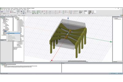
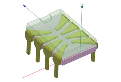
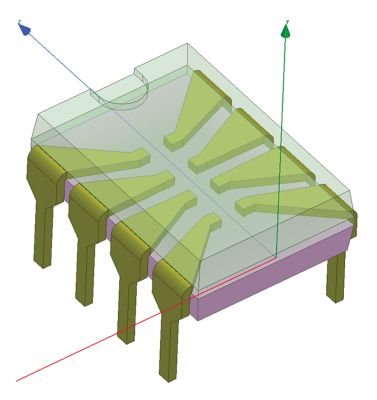
Virginia Tech students use Ansys Electronics Desktop to load a transistor outline package into Q3D Extractor.
Fundamentally, a package provides four things for the electronics embedded within:
- Protection from environmental variables, such as humidity, heat, chemicals and corrosion
- Interconnection of electrical signals
- Power distribution to the electronic devices and circuits
- Thermal management, ensuring that heat is dissipated away from the semiconductor devices within the package so that they can operate reliably and efficiently throughout the lifetime of the device
VA Tech students use Ansys Q3D Extractor to verify their calculations to determine DC resistance and DC inductance of various paths and components in the package.
Over time, as these chips have grown more efficient, manufacturers have discovered that they can shrink the size of the chip without increasing the heat produced by the components themselves. As a result, the chips end up creating the same amount of heat, but it is concentrated in a smaller area, increasing the heat flux. From an engineering design perspective, this creates a real multiphysics challenge: How can you optimize the design of the electronics package to enable optimal performance of the components within while optimizing the dissipation of heat? The answers are bound up in a complex interplay of electrical engineering (EE), mechanical engineering (ME) and materials science (MS) — and what might appear to be the best answer from an EE perspective may not necessarily appear to be the best answer from an ME or MS perspective. Nor might any of these individual answers be the best answer when considered in light of the usage scenario for which the package is intended.
Moreover, heat flux is only one of the challenges that engineers face as the forms get smaller. Another arises from the proximity of the elements within the package. Every real-world element (as opposed to a theoretically perfect element) has what are known as parasitic qualities — a parasitic inductance or a parasitic resistance, for example — that produce unintended effects, such as a ringing that can affect the switching of the semiconductor device itself. Such parasitic qualities are inherent in a conductor, and they can be readily calculated for any individual component. However, when you pack more and more conductors next to one another in a smaller form, the parasitic qualities of each individual element interact to create a new effect that is different from — and not just the sum of — the individual parasitic effects. Sometimes the compounded effects are beneficial; other times they are detrimental. How do you know which it will be? You test. You analyze. You refine.
GAINING INSIGHTS WITH ANSYS
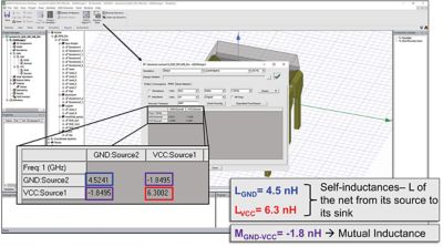
Simulation software from Ansys is key to helping students in ECE 4984/5984 gain insights that can help them understand all these dynamics and, in turn, help them learn how to approach the multiphysics challenges inherent in electronics packaging. In one assignment, teams of students analyze the electrical and thermal performance of a transistor outline (TO) package, which is a standard package for power electronics. The first part of the project requires them to perform a series of calculations to determine DC resistance and DC inductance of various paths and components in the package. They’re asked to identify which path has the largest resistance and which loop has the largest inductance — and then to explain their answers, based on their calculations. Then they’re asked to identify which component contributes most resistance to the gate path and the drain path, which component contributes the most inductance to the power loop and so on — and to justify their conclusions using the values they have calculated. Ultimately, I ask them to explain how the DC resistances and inductances could be reduced and to speculate on what effect their changes would have on package performance.
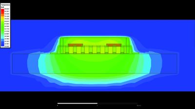
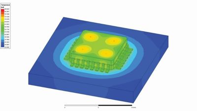
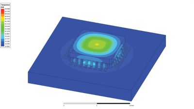
VA Tech students use Ansys Icepak to create temperature plots of the quad flat package (QFP) with four smaller die and mold material for the package.
Then they load the TO package into Q3D Extractor to verify their findings. It is always interesting.
In the software, they’re asked to identify and explain the differences between their calculated results and those shown by the electromagnetic field simulations presented in Q3D Extractor. We’ve spent one to one and a half class periods learning how to use the software, so they’re ready for this. Those differences they discover are sometimes dramatic, and I want them to figure out how the discrepancies arose. Sometimes the smallest things — not taking into account a bend in a lead, for example — can lead to a significant difference between the calculated value and that arising from simulation. Then they’re asked to simulate AC resistances and inductances using Q3D Extractor and to answer a number of questions about how the AC and DC values compare. What students can learn from Q3D Extractor in just 10 minutes — for that’s all it takes, even on their personal computers, to perform a TO electromagnetic field simulation — is eye-opening for them. In many cases, the software verifies what they thought they knew while in other cases it exposes things they hadn’t fully taken into consideration. Q3D Extractor provides them with a way to explore alternatives quickly and to see how subtle changes ripple throughout the fabric of a package.
ADDING ICEPAK ANALYSIS
As part of this team project, students also use Icepak to gain greater insight into the thermal characteristics of the TO package. As before, they’re asked to calculate a number of results in advance. Where do they expect the most heat to be dissipated on the TO and why? Which path will have the lowest thermal resistance and which component will cause the greatest resistance in that path? How could that be reduced?
Once they have calculated answers to these questions and spent another class period learning how to use Icepak, they load the TO model and run thermal simulations to validate their answers. Again, this is always insightful for rarely is there a perfect match between what a student expected and what the simulation software shows.
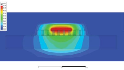
VA Tech students can use Ansys Icepak to compare various temperature plots of the QFP. Shown here are temperature plots of the QFP with the leads.
They then run a variety of simulations to explore the answers to other questions. What is the maximum junction temperature for each die? Where on the package does the greatest amount of heat transfer take place? Was that where it was expected? Where is the least amount of heat transfer taking place and what could be done to the package to improve heat removal?
With the tools from Ansys, the answers to these questions are readily accessible. The 3D heatmaps provide far more insight than the 1D and 2D insights that typically arise from manual calculations. It becomes easy to see how the thermal dynamics and the materials used in the packaging design affect its electrical characteristics and performance. Similarly, it becomes easy to see how the electrical characteristics of the components inside the package can affect the materials and the thermal characteristics of the package itself. Indeed, what they gain is insight into a multidimensional, multiphysics interaction that often goes beyond what they’ve encountered in other classes.
A WORLD OF COMPLEX INTERACTIONS EXPOSED
In looking at the physics of a tiny little chip, students from across the engineering discipline — from electrical engineering to mechanical engineering to materials sciences — see a world of interactions and variations that force them to start looking at the practical application of their disciplines in a new way. The concepts and technologies they’re focusing on within their undergraduate or graduate tracks — the electrical characteristics of an integrated circuit or the physical properties of different materials — don’t exist in a vacuum. Physics doesn’t stop at the edge of their discipline.
Teams of VA Tech students use Ansys Electronics Desktop and Ansys Icepak to analyze the electrical and thermal performance of a transistor outline (TO) package.
Accordingly, we focus on the multiphysics that integrate electrical engineering, mechanical engineering and materials sciences. There are not many other courses where we can look at the interplay of all these disciplines and their physics at the same time, but it really is an important lesson for those students who are keen to leave school and get a job in industry, particularly if they take positions in companies that are incorporating electronics packaging into the products they are building.
So far, the engineering students at Virginia Tech seem to agree on its value. The first year I taught this course, I had hoped to enroll as many as 10 students — but demand was such that I ended up enrolling 15 students. The next year that I taught the course, nearly 40 students enrolled. We’re taking complex, real-world projects, breaking them down into small pieces, and then using powerful tools like those from Ansys to help us