-
-
Kostenlose Software für Studierende
Ansys unterstützt die nächste Generation von Ingenieur*innen
Studenten erhalten kostenlosen Zugang zu erstklassiger Simulationssoftware.
-
Verbinden Sie sich jetzt mit Ansys!
Gestalten Sie Ihre Zukunft
Stellen Sie eine Verbindung mit Ansys her, um zu erfahren, wie Simulation Ihren nächsten Durchbruch vorantreiben kann.
Länder und Regionen
Kostenlose Demoversionen
Produkte & Dienstleistungen
Lernportal
Über das Unternehmen
Back
Produkte & Dienstleistungen
Back
Lernportal
Ansys unterstützt die nächste Generation von Ingenieur*innen
Studenten erhalten kostenlosen Zugang zu erstklassiger Simulationssoftware.
Back
Über das Unternehmen
Gestalten Sie Ihre Zukunft
Stellen Sie eine Verbindung mit Ansys her, um zu erfahren, wie Simulation Ihren nächsten Durchbruch vorantreiben kann.
Kostenlose Demoversionen
ANSYS BLOG
December 18, 2020
System-Level Electromagnetic Simulation: It’s Within Your Reach
The digital revolution has placed incredible pressure on engineering teams to produce new, high-performance printed circuit boards (PCBs) and chip packages rapidly. However, as data rates continue to grow exponentially and designs become ever-smaller, with ever-greater outputs, the likelihood of signal degradation due to discontinuities and unwanted signal coupling is increasing. Despite market pressures, design validation can’t be shortchanged.
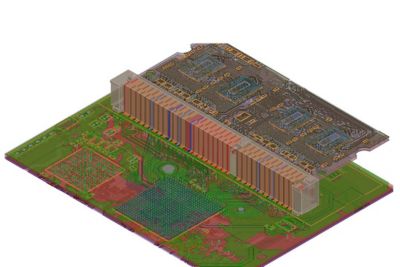
This 3D model of a complex PCB package was generated and
solved in just 34 hours using Ansys HFSS
Historically, verifying chip-to-chip system-level performance has involved a series of electromagnetic (EM) simulations at the component level. For example, engineers conduct simulations to confirm the signal integrity of a single ball grid array (BGA) package, from solder bump to solder ball ― or to confirm signal integrity from an integrated circuit (IC) footprint, through trace routing, to a connector footprint.
When all the individual pieces of the system are simulated and validated, they’re assembled into a physical prototype. The problem with this serial approach? First, it’s time-consuming, often delaying launch dates. Second, signal discontinuities caused by component integration and other system-level issues are only identified during the prototype phase, resulting in the high costs and additional delays associated with rework.
In the past, this sequential approach has represented a significant product development hurdle for semiconductor manufacturers. Older simulation approaches, computing resources, processing speeds and engineering methods limited engineers to using this serial, component-level approach.
Capitalize on Fast, System-Level EM Simulation ― with Your Existing Tools
The good news is that Ansys HFSS simulation software has the capabilities to support rapid system-level virtual prototyping for PCBs and chip packages. Matched with today’s elastic cloud computing resources, faster processing cores, rapid data transfer speeds and other innovations, HFSS is accelerating electromagnetic (EM) simulation.
While many Ansys customers aren’t yet aware of the system-level simulation capabilities in HFSS, semiconductor leaders are already leveraging them to achieve speedups of 10x to 12x in their EM simulation run times for complex products. These kinds of speed improvements require no additional software investment for existing Ansys 2020 R2 customers. Engineering teams just need to apply the full capabilities of the newest HFSS solution in an optimized technology environment, using best practices resulting from more than 30 years of experience.
As just one example, consider a PCB design that incorporates eight two-layer flip-chip BGA packages mounted on a SODIMM board, plugged into a connector that is mounted on a motherboard. In total, 64 nets were simulated and 128 ports were defined.

Ansys HFSS offers system-level capabilities that bring all package
components together in a single, connected 3D model
― replacing a slow, outdated serial approach to EM simulation
Validating this complex product design, with all its integration points and components, would take weeks via yesterday’s sequential, component-level approach. But, by applying HFSS in a best-practice, system-level manner, a full 3D model of this large PCB module was generated and solved in only 34 hours.
This is the level of speed and performance electronics companies need to achieve today ― and it’s within easy reach for engineering teams using Ansys 2020 R2. By capitalizing on the system-level capabilities in HFSS, companies can introduce more complex designs and support risk-taking and innovation, while achieving enormous savings in development time and costs, compared to previous validation methods.
Streamline the PCB Assembly Process, with No Surprises in Production
For the first time, HFSS enables the virtual assembly and validation of all PCB and chip package components in a risk-free simulation environment. This easy-to-use solution can directly read electrical computer-aided design (ECAD) layouts ― including boards, packages, connectors and single inline packages (SiPs) ― and virtually assemble them. HFSS can also import mechanical computer-aided design (MCAD) elements, including their boundary conditions, port excitations and material properties.
Engineering teams can quickly solve a fully coupled system in a virtual design space, including both MCAD and ECAD domains, capturing system-level performance at the earliest possible stage ― when the costs of rework are minimal. HFSS not only streamlines the system assembly and physical prototyping processes, but it helps avoid later manufacturing problems, product recalls and warranty claims.
Because HFSS is tightly linked to other Ansys solutions, the solved model can be seamlessly passed on to other Ansys solvers for additional analysis. Thermal and structural solvers can help ensure that the final product package is managed for heat effects, as well as designed for real-world environmental conditions. This tight integration positions product development teams to capitalize on more than 50 years of Ansys engineering simulation leadership across multiple physics.
Ansys has many resources available to help customers understand and leverage the system-level capabilities of HFSS. These include a wide range of free, on-demand Ansys Innovation Courses and targeted EM simulation training at the Ansys Learning Hub. The Learning Hub offers three different HFSS 3D layout courses, available online 24/7. Ansys customers can also reach out directly to their account team or access online support at any time.