There is no doubt about the rapid advancement of modern devices and their components, but how are engineers adapting to keep up? Designing analog and mixed-signal (AMS) semiconductor circuits is as much an art as it is a science. As we look to the future, we can anticipate that these advancements will bring forth exciting challenges and opportunities for engineers, pushing the boundaries of creativity and technical expertise.
In semiconductor engineering, the complex nonlinear interactions of electromagnetic fields with silicon are difficult to predict, and the challenges created by these interactions increase dramatically with advanced manufacturing processes at 16 nm and below. It is important to understand why these challenges exist and what designers must do to reliably design analog circuits with leading-edge nodes.
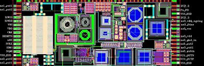
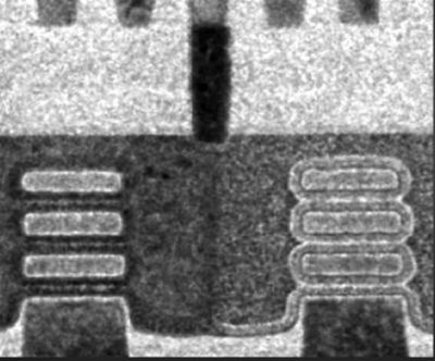
Layout of a voltage-controlled oscillator (VCO), which is an analog structure found on most digital ICs.
How Parasitics Impact Chip Manufacturing
From the earliest days of the semiconductor industry, making accurate predictions by modeling and simulating analog effects has proven extremely valuable. The SPICE circuit simulator, widely used by semiconductor engineers, is a foundational tool for any analog chip design. However, analog design still requires a degree of expertise and engineering judgment, both of which are essential to success.
The accuracy of a SPICE simulation depends on the circuit models provided, as real-world effects and interactions are difficult to replicate. Transistor elements must be characterized with considerable care and effort, as documented in the process design kit (PDK) libraries provided by the semiconductor foundry. However, extracting models of the on-chip interconnect parasitics must be quick and easy for every layout iteration, as their influence on circuit performance increases as manufacturing nodes shrink and operating frequencies increase. The impact of interconnect parasitics on circuit performance has become so strong that accurate modeling of electromagnetic, radio frequency (RF), thermal, optical, parasitic, voltage drop, reliability, power, and other multiphysics has become vital to a successful design.
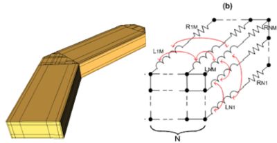
A section of semiconductor interconnect with its extracted electromagnetic model from Ansys RaptorX software, including full inductive coupling. The finite element mesh is created automatically to represent the physical layout for the simulator.
Consequently, most analog design teams opt to use mature process nodes, which are far removed from the challenges of designing with leading-edge silicon. Advanced silicon is not only more costly to produce, but it primarily benefits only digital designs. Criteria like integration density and switching speed take precedence over analog design concerns such as linear behavior and predictable interactions. Given the choice, most analog designers prefer to avoid the latest advanced fin field-effect transistor (finFET) and gate-all-around (GAA) transistor technologies because these make their design jobs harder. Electrical behaviors at these nodes become less predictable and more sensitive to interference from surrounding elements. Also, the benefits in the areas of lower power and greater integration density are not as relevant for analog designs.
Electromagnetic Modeling Needed for Accuracy
Analog design with advanced nodes is unavoidable for larger system-on-chip (SoC) components that integrate all the electronic elements of the system onto a single advanced-node chip. This has been an advantageous trend in semiconductor design for several decades. Subsequently, every SoC contains some analog subcircuits that will share the same advanced process technology as the rest of the design. Also, the analog content on advanced-node chips has grown due to product trends like the need for integrated sensing; wireless communications like WiFi, Bluetooth, and 5G; and greater reliance on video and touchscreens. To be successful, analog designers need electromagnetic simulators to extract accurate resistance, inductance, and capacitance (RLC) or S-parameter models for the analog interconnect on an SoC.

Intel’s advanced silicon manufacturing technology includes RibbonFET gate-all-around transistors and PowerVia technology that relocates the power distribution network from the front side to the back side of a chip. These innovations introduce new multiphysics analysis challenges as they shrink the size of chips, improve their performance, and reduce voltage losses.
Did you know?
Within all electronic devices lies at least one, but typically multiple, integrated circuits (ICs) — commonly called chips — made from silicon. Increasingly, analog and mixed-signal (AMS) chips are expanding in use because they seamlessly integrate analog with digital signals on a single chip design. By ensuring smooth communication between analog circuits and digital processors, AMS chips are crucial to powering cellular and wireless devices, electric vehicles (EVs), Internet of Things (IoT) networks, and other applications.
Engineers simulate their ICs in great detail with physics-based simulation software before sending the design off to a silicon foundry, known as a “fab,” for manufacturing. It can take three to four months and millions of dollars to manufacture a batch of chips, and they cannot be repaired or altered in the event of an error. This is why it’s vital for designers to make sure the chip will work correctly through means like simulation software before they commit to manufacturing.
Circuit layouts with advanced process nodes introduce many physical effects that pose significant challenges for accurate electromagnetic analysis. Smaller geometries lead to closer physical spacing, higher electromagnetic coupling, and higher resistance, which can all make the performance of analog circuits much more sensitive to precise details of the physical layout.
Understanding Layout-Dependent Effects
More importantly, there is a large set of manufacturing effects that make it more challenging to use traditional modeling techniques for advanced nodes. These are collectively referred to as layout-dependent effects (LDE). LDE effects like etching, multi-patterning, conformal dielectrics, damage, and loading must be analytically calculated to produce an accurate electromagnetic model. However, many traditional electromagnetic modeling tools do not support LDE and can give inaccurate results at advanced nodes. Benchmarks have shown that ignoring advanced LDEs can result in high levels of model inaccuracy — for instance, measurements can be up to 140% off in series resistance and up to 25% off in total capacitance.
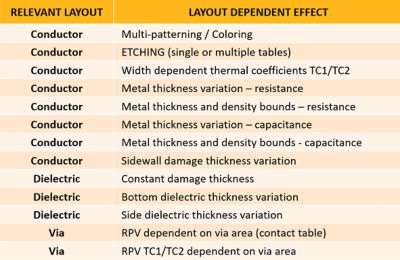
An overview of layout-dependent effects (LDE) that affect the electrical behavior of semiconductor circuits implemented on advanced technology nodes.
A more comprehensive list of common LDEs is shown in the table above. This illustrates how manufacturing process steps such as etching and planarization result in varying electrical and thermal parameters for conductors, dielectrics, and vias. For example, when all three dielectric effects are considered, total capacitance could increase by 10% in some applications. This illustrates how important it is for designers to accurately account for LDEs.
An advanced nano-sheet transistor structure manufactured by TSMC exhibits layout-dependent effects (LDE) that must be included for accurate analysis of analog circuits. Photo courtesy of TSMC
A Solution for Advanced Nodes
Ansys has collaborated with leading silicon foundries to enable the Ansys RaptorX silicon-optimized electromagnetic solver for advanced-node LDEs. The RaptorX solver can fully model all LDEs in advanced complementary metal–oxide–semiconductor (CMOS) process nodes down to 2 nm and below. RaptorX software can use encrypted PDK files to access the LDE parameters for a specific process node while still protecting the foundry’s intellectual property (IP).
Accurately accounting for advanced process node effects and LDEs greatly increases simulation accuracy and reliability. Advanced simulation engines like RaptorX software make it possible to design high-speed analog components on SoCs that take advantage of the newest silicon process nodes. Including these effects in RaptorX calculations is automatic and requires no change to existing extraction flows.
Download the Optimizing Analog Design with Multiphysics e-book and visit the Ansys website to learn more about the Ansys Semiconductor product collection.
Just for you. We have some additional resources you may enjoy.


The Advantage Blog
The Ansys Advantage blog, featuring contributions from Ansys and other technology experts, keeps you updated on how Ansys simulation is powering innovation that drives human advancement.