Synopsys and Ansys power the future of innovation—connecting silicon to systems.
ANSYS BLOG
September 05, 2019
Mitigate BGA and QFN Failures Using Redesigns, Underfills, Edge Bonds or Corner Staking
Ball grid array (BGA) and quad flat-pack no-lead (QFN) are among the most prevalent packages for integrated circuits (ICs). The challenge is that BGAs and QFNs present a greater risk than their leaded counterparts for solder joint failure.
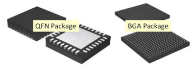
A QFN and BGA package
These solder joint failures occur because BGAs and QFNs are susceptible to:
- Thermal cycling
- Vibration
- Mechanical shock
- Weak board connections
So, why the popularity? BGAs and QFNs are more powerful and less expensive than leaded packages. As a result, they are incorporated into a wide range of technologies. In fact, BGAs generate about two-thirds of semiconductor packaging revenue. QFNs, on the other hand, are the most popular IC package by volume.
Clearly, BGAs and QFNs aren’t going anywhere anytime soon. So, designing products without them isn’t a viable way to mitigate the risks these packages present. Alternatively, there are two methods to address potential failure:
- Using underfilling, edge bonds and corner staking to reduce solder joint strain
- Using reliability physics analysis (RPA) analysis to change BGA and QFN designs
Both solutions are comprehensive, so let’s break them down.
When to Minimize BGA and QFN Failures with Underfills, Edge Bonds and Corner Staking
As a risk mitigation measure, underfilling, edge bonds and corner staking can be cost effective — compared to the varying costs associated with redesigning BGAs and QFNs.
However, solving BGA and QFN failure after the component designs are determined — as is often the case — is a band-aid fix.
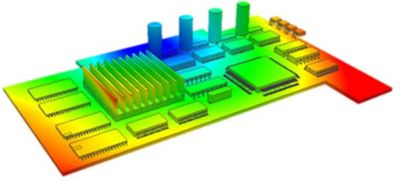
ANSYS Sherlock mechanical cycling simulation of a board
Sometimes band-aid fixes, like underfilling, are exactly what’s needed to mitigate risk without incurring package redesign expense. However, underfilling is a time-consuming process with expensive materials. As a result, underfilling is a good solution only for small quantity runs of BGAs. In high-throughput scenarios with lower cost targets, edge bonds and corner staking are better choices.
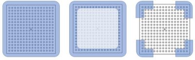
BGA and QFN failures can be mitigated using underfill methods.
Engineers can select the optimal underfill method based on prior knowledge of the dominant failure mechanism. Underfilling the full area, perimeter or edge bonding offers a different level of mitigation depending on the underfill behavior, loading condition and electronic package type.
In fact, some combinations of underfill material and application type have been shown to reduce reliability performance under thermal cycling while improving performance under mechanical shock. In other words, engineers need to know how their band-aid fixes could result in adverse thermal cycling and mechanical cycling issues.
Unlike lead packages, temperature cycling impacts solder joints and mitigates the performance of BGAs and QFNs. To solve these issues, engineers can use:
- Underfilling
- When engineers can balance the glass transition temperature (Tg), coefficient of thermal expansion (CTE) and elastic modulus (E).
- Corner staking
- When engineers need to use less material, in high throughput situations.
- When the lowest expense and risk are required; however, these improvements are limited in high or low temperatures.
- Edge bonds
- When engineers need a similar solution to corner staking with an improved time-to-failure.
As with thermal cycling, underfilling, edge bonds and corner staking present mechanical cycling challenges. Engineers should keep track of:
- Shock testing which often causes solder joint failures
- Vibration testing in cold environments which increased the failure rates of all mitigation techniques
To learn more, watch the webinar: The Reliability of BGAs, QFNs and Other Critical Packages.
Using RPA to Optimize BGA and QFN Designs
Underfilling, edge bonds and corner staking are viable remedies for BGA and QFN failure. However, none of these options offer a complete solution.
To completely solve the problem, engineers can optimize the BGA and QFN designs using RPA and Ansys Sherlock’s automated design analysis capabilities.
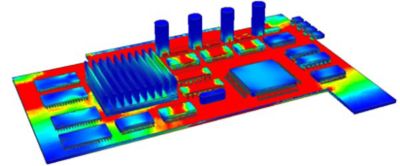
ANSYS Sherlock mechanical cycling simulation of a board
Sherlock can be used to predict the lifetime of a solder joint. When the BGA and QFN undergo thermal cycling, the different expansion and contraction behaviors of the solder and materials cause stress and strain. These forces deform the solder.
The extent of the strain dictates the lifetime of the solder joint — the higher the strain, the more the solder joint is damaged and the shorter the lifetime. Sherlock uses physics-based degradation algorithms to predict vibration and mechanical shock performance over a range of temperatures, not just the standard 25 C (77 F) for electronics. The virtual tool also develops predictive models and design rules based on critical drivers like:
- Component and board CTE and elastic modulus
- Component length
- Solder volume and thickness
- Solder fatigue properties
Based on these critical drivers and physics-based degradation algorithms, engineers can estimate the strain energy dissipation in the BGA and QFN. Sherlock bases its time-to-failure predictions on strain energy. It enables engineers to make design adjustments, before layout — saving time and money while extending time-to-failure and meeting reliability goals.
Engineers can optimize the use of RPA following this three-step process:
- Implement RPA during component engineering or parts selection.
- Assess risk of solder joint failure for each new component.
- Benchmark RPA prediction
- Run an RPA simulation and compare it to the supplier’s test environment.
- If lacking test data, identify reliability by similarity (RBS) then test or use RPA only.
- Once the component passes RPA in RBS, test it in the designed package.
- Perform RPA before layout
- Running RPA after layout is moot because it’s too late to make design changes.
Traditionally, RPA strategies take time. However, Sherlock is able to translate electronic computer-aided design (ECAD) and mechanical computer-aided engineering (MCAE) data into 3D finite element models. This democratizes the thermal and mechanical analysis of electronics. As a result, BGAs and QFNs can be optimized in hours instead of weeks.
To learn more about reliability physics analysis, join the webinar Introduction to Reliability Physics Analysis.