Synopsys and Ansys power the future of innovation—connecting silicon to systems.
-
-
Access Free Student Software
Ansys empowers the next generation of engineers
Students get free access to world-class simulation software.
-
Connect with Ansys Now!
Design your future
Connect with Ansys to explore how simulation can power your next breakthrough.
Free Trials
Products & Services
Learn
About
Back
Products & Services
Back
Learn
Ansys empowers the next generation of engineers
Students get free access to world-class simulation software.
Back
About
Design your future
Connect with Ansys to explore how simulation can power your next breakthrough.
Free Trials
TOPIC DETAILS
What is a Waveguide?
Waveguides are specialized structures that guide electromagnetic waves from one location to another and are often used to connect two or more components for information transfer. Waveguides are typically rectangular or circular in cross section and guide microwaves, radio waves and light waves (optical waveguides) with low loss.
Many factors affect how waveguides propagate different electromagnetic waves, including:
- Waveguide shape
- Waveguide size
- Characteristics of the materials used, such as rigidity or flexibility
Waveguides are often confused with coaxial cables because both are transmission lines for guiding electromagnetic waves. However, the structure and propagation methods of waveguides differ from coaxial cables. Coaxial cables use two conductors separated by an insulating material to propagate electromagnetic waves, whereas inside a waveguide, electromagnetic waves travel and propagate inside a hollow structure that supports different “modes.” Optical waveguides use the difference in refractive index between two materials to ensure that light waves propagate to their intended destination. Non-optical waveguides, used in applications like microwaves, confine and guide electromagnetic radiation using impedance or material conductivity to guide the waves.
In this article, we taken an in-depth look at what waveguides are and how different types are used today, with a strong focus on optical waveguides.
What is an Optical Waveguide?
Optical waveguides transport light at different optical frequencies ― often in the infrared range ― and are commonly used to route or control optical signals.
The most common type of optical waveguide is the optical fiber used in optical communications. Optical fibers are conventionally made of silica glass and have a high refractive index core and low refractive index cladding to guide light along the fiber.
Less common are planar optical waveguides. These are known as on-chip waveguides because the optical waveguide is fabricated on top of semiconductor chips such as silicon-on-insulator, gallium arsenide, lithium niobate, or indium phosphide. On-chip waveguides can have a number of geometries, including rib, strip, microstrip, loaded, inverted rib, and photonic crystal.
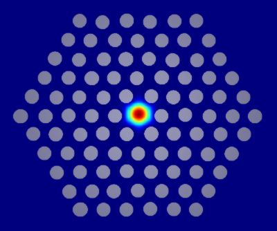
A photonic crystal fiber
Photonic crystals are an emerging area of optical waveguide because they behave differently than other waveguides. Instead of guiding light by the refractive index of the waveguide, light is guided by the patterning of the photonic crystal, as light can’t travel through the crystal itself. Certain wavelengths of light are blocked by the crystal’s photonic band gap , similar to an electronic band gap in semiconductors. Photonic crystals are essentially “optical semiconductors.”
Types of Optical and Non-Optical Waveguides
There are many types of waveguides, including optical waveguides and waveguides used for guiding microwave frequency, radio frequency (RF), and other electromagnetic waves.
Circular Waveguides
Circular waveguides are hollow tubes primarily used to guide microwave and radio waves in transverse electric (TE) and transverse magnetic (TM) modes. The waves are guided along a circular path, often via metallic waveguides.
This class of waveguide is commonly used in wireless communications, microwave backhaul, and radar applications.
Coplanar Waveguides
Coplanar waveguides are rectangular waveguides that have conductors with a central conducting strip and two ground planes, with all the conductors located on the same side of a substrate material (such as a printed circuit board, or PCB). Coplanar waveguides are used to guide microwaves in microwave devices, millimeter-wave (mmWave) circuits, and monolithic microwave integrated circuits (MMICs).
Flexible Waveguides
Flexible waveguides differ from other waveguides because they can twist and bend to fit into constrained spaces that more rigid waveguides cannot. Flexible waveguides are made of copper, brass, or aluminum with a flexible outer layer and may include corrugated and helical structures to provide flexibility. However, these may also introduce resistance and signal attenuation into the waveguide.
Flexible waveguides come in three main forms: twistable, bendable, and flexible-twistable. They are largely used in microwave-guiding applications in the communications and aerospace sectors.
Zero-Mode Waveguides
Zero-mode waveguides (ZMWs) are optical waveguides that guide light into small volumes below the wavelength of light. They use nanoscale structures, such as tiny apertures that reduce the optical observation volume, to achieve this confinement.
Unlike other optical waveguides, ZMWs do not support propagating optical modes and are instead used in plasmonics, quantum optics, and single-molecule or fluorescence imaging.
Dielectric Waveguides
Dielectric waveguides are the cylindrical waveguides used to construct optical fibers and on-chip waveguides. Dielectric waveguides have a high refractive index core and low refractive index cladding. The light waves propagate using the principle of total internal reflection: when light attempts to move from a denser medium to a less dense medium, it is reflected back into the denser medium at the material interface. The guided waves are thus trapped in the fiber core, which makes transmission over long distances with low loss possible. Dielectric waveguides are widely used in optical communications and integrated optics.
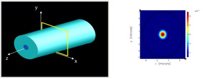
Simulation of dielectric waveguide
The Different Waveguide Modes
All waveguides propagate electromagnetic waves through modes. In optical waveguides, the mode refers to the shape light takes as it travels down the waveguide. Smaller waveguides have fewer modes, but larger waveguides support more modes of propagation. For optical modes, a consistent cross section throughout the waveguide is crucial, as any changes can cause scattering that influence attenuation (loss of signal) within the waveguide.
Transverse Electric and Transverse Magnetic Modes
Transverse electric (TE) and transverse magnetic (TM) modes are two common waveguide modes used to propagate microwaves. A mode that combines both is known as a TEM mode. These modes can also occur in optical waveguides.
Both TE modes and TM modes are defined by the direction of the electromagnetic field during propagation. Electromagnetic fields are vectors that point in a specific direction at a given time. In TE modes, the electric field is transverse (perpendicular) to the direction of wave propagation (either horizontally or vertically). In TM modes, the magnetic field is transverse to the direction of propagation. Optical waveguides can use quasi-TE and quasi-TM modes, which are approximations of TE modes or TM modes, unlike those in microwave or radio-wave propagation.
Single-Mode vs. Multi-Mode Fibers
In optical fiber waveguides, light can propagate in either single mode or multi-mode. Single-mode fibers have a very small core, whereas multi-mode fibers have a much larger core. Single mode fibers are used in silicon photonics and long-range optical communications because their smaller core supports a smaller number of modes, therefore enabling light (and the information contained within it) to travel efficiently over long distances. However, because of the smaller core, it’s harder to get light into the waveguide. Specialist lasers and optical components are required to pulse the light into the fiber.
Multi-mode fibers aren’t suited for long-range telecommunications because the presence of more than one mode causes the light pulses to travel and spread out at different speeds. Multi-mode fibers are better suited to short-range communication networks, such as local area networks (LAN) and data centers.
Examples of Waveguides in Action
There are many uses of waveguides (both optical and non-optical), including:
- Optical communications (telecommunications)
- Photonic integrated circuits (PICs)
- Optical sensors
- Lasers
- Interferometers
- Radar
- Microwave and RF communications
- Printed circuit boards (PCBs)
- Optical circuitry
- Optical transmitters
- Terahertz (THz) communications
- Mixed-reality systems such as augmented reality (AR) and virtual reality (VR), which use larger waveguides (called lightguides) that are distinct from conventional waveguides
Optical Communications
Optical communications is one of the largest commercial application areas that uses dielectric waveguides to guide light from one location to another, carrying information between systems. Single-mode fibers are used for long-range communication, while multi-mode fibers are used for short-range communication.
Semiconductor lasers generate light pulses that carry encoded information to the fiber. The information is encoded on the optical signal either by modulating the laser’s driving current or with external modulators that are separate from the laser. The wave then travels through the fiber until it is received by a waveguide receiver, which includes a photodiode and a transimpedance amplifier. These receivers process high-frequency optical signals from the fiber into an electrical signal to enable data transmission.
The material properties of the optical waveguide are important. Outside of the appropriate refractive indexes, a material’s absorption characteristics are also important, as too much optical absorption can result in signal loss. Because of this, waveguides are transparent and made with glass or clear plastics. Opaque cladding materials would absorb too much light and cause excessive attenuation in the fiber.
While most optical communications (e.g., telecommunications) use waveguides, not all optical communication technologies require them. A key example is free-space optical (FSO) communication, which propagates light through air (i.e., free space) to send data between a transmitter and receiver.
Photonic Integrated Circuits
Optical waveguides are also used in photonic integrated circuits (PICs) as the “wires” of the circuit. They are synonymous with conventional wires in electronic integrated circuits (ICs), but they transmit signals via light rather than electrons. The waveguides are used to connect different components on the PIC.
PICs are often coupled to optical fibers using components like lenses to change the focus of the light, as optical fibers have a much larger mode size than PICs. So, the light is focused to a smaller scale to reduce losses.
There are many PIC components that use waveguides. These include:
- Splitters: split the light wave from a single waveguide into two waveguides
- Couplers: couple the light waves from two different waveguides into a single waveguide
- Ring resonators: consist of circles or ovals that can be used as filters or modulators on the PIC
- Spiral waveguides: delay the signal on the PIC
- Grating couplers: couple light vertically from the chip into and out of optical fibers
- Optical switch: change the refractive index within a waveguide to control and route optical signals around the PIC
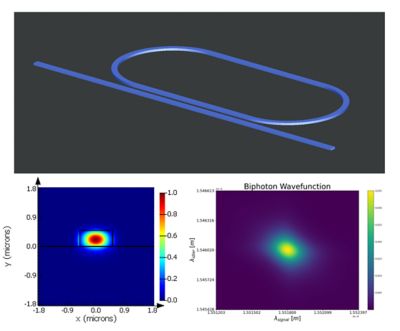
Simulation of microring resonator in a photonic integrated circuit (PIC)
Optical Sensors
Optical waveguides are widely used in optical sensors. In chemical sensing, the presence of a gas or liquid molecule produces a detectable response. The molecules bond with or cause interference to the waveguide, which changes the refractive index across the waveguide. This can then be measured and quantified to determine the chemical species of interest. Other common applications that use optical waveguides include light detection and ranging (lidar), vision sensors, and fiber-optic sensors.
Fabricating Optical Waveguides
Optical waveguides are fabricated with techniques like:
- Lithography
- Laser writing
- Thin-film deposition
- Fiber drawing
- Direct-write techniques
For on-chip optical waveguides, the semiconductor chips are created using the same semiconductor fabrication techniques that are used to make conventional IC chips. This includes:
- Photolithography
- Plasma etching
- Reactive ion etching (RIE)
- Chemical vapor deposition (CVD)
- Metal organic CVD (MOCVD)
- Physical vapor deposition (PVD)
- Atomic layer deposition (ALD)
- Molecular beam epitaxy (MBE)
Accuracy in the fabrication process is vital because surface roughness in a waveguide can cause scattering and optical loss. Like any semiconductor, both the fabrication process and environment are crucial to maintaining high sensitivity and preventing contamination.
Designing and Simulating Waveguides
Waveguides can be simulated and their modes predicted using mode solvers. The Ansys Lumerical product collection helps engineers simulate optical waveguides, and Ansys HFSS high-frequency electromagnetic simulation software can be used for RF and microwave simulations. Simulation can help engineers to better design waveguides without the need for extensive trial-and-error prototyping.
Here are examples of what can be achieved with simulation software:
- Designing different types of waveguides that are made from a range of materials and across several sizes
- Optimizing the X and Y waveguide cross sections (for example, propagation is in the Z direction)
- Calculating which modes ― TE mode, TM mode, single mode,or multi-mode — will be used in a waveguide
- Calculating the propagation constant and effective index of a waveguide mode as light travels along it
- Calculating the electric field profile of a waveguide, including the X, Y, and Z components of the field
- Checking that propagating waves will have no interference
- Calculating potential loss, including losses that may arise from the bending of waveguides
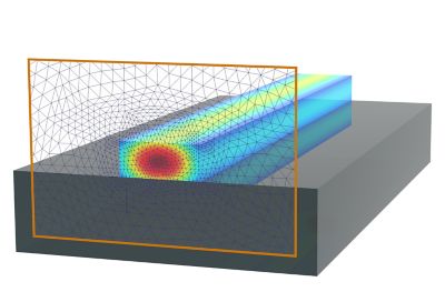
Simulation of a rectangular waveguide
Along with investigating the properties of the waveguides, the systems they are integrated into can also be simulated to develop better on-chip designs.
For example, engineers can use simulation to examine waveguides as modes propagate down the waveguide. They can see how light behaves at splitters or couplers to ensure that the light is coupled or split efficiently and minimize loss within the larger optical or photonic system.
When designing optical circuits, engineers can also use simulation to analyze other components and ensure they have the optimal properties, functionalities, and characteristics for the intended application.
Get in touch with the Ansys technical team today to discover how simulation can help you design and optimize advanced waveguides.
Related Resources
Let’s Get Started
If you're facing engineering challenges, our team is here to assist. With a wealth of experience and a commitment to innovation, we invite you to reach out to us. Let's collaborate to turn your engineering obstacles into opportunities for growth and success. Contact us today to start the conversation.