-
-
Access Free Student Software
Ansys empowers the next generation of engineers
Students get free access to world-class simulation software.
-
Connect with Ansys Now!
Design your future
Connect with Ansys to explore how simulation can power your next breakthrough.
Free Trials
Products & Services
Learn
About
Back
Products & Services
Back
Learn
Ansys empowers the next generation of engineers
Students get free access to world-class simulation software.
Back
About
Design your future
Connect with Ansys to explore how simulation can power your next breakthrough.
Free Trials
ANSYS BLOG
April 15, 2021
Ansys and GLOBALFOUNDRIES Team to Accelerate Photonic Integrated Circuit Design
Ansys has teamed up with GLOBALFOUNDRIES© (GF©), the world’s leading specialty semiconductor manufacturer, to address the needs of the digital world through integrated photonics design.
GF enables designers to leverage the power of light for advanced optical applications with a high-performance monolithically integrated photonics solution in an optimized footprint that requires only half the area of discrete solutions. This monolithic solution integrates a high performance RF CMOS and photonics components in a single chip to deliver higher bandwidth between data center servers and faster connections between data centers along the telecommunication infrastructure.
With its silicon photonics (SiPh) technologies and advanced packaging capabilities, GF enables high-performance optical connectivity designed to keep pace with the demands of metro, long haul and intra/inter data center applications, while maximizing reach and energy efficiency.
With its Lumerical photonic simulation tools, Ansys enables designers to understand light and predict how it behaves within complex structures, circuits and systems. Ansys enables our customers to establish a leading position in the development of transformative technologies employing photonics.
This new collaboration delivers key capabilities including a process-enabled custom design and Verilog-A circuit simulation enablement through accurate simulation results, model compatibility and comprehensive model libraries.
Foundry-Compatible Custom Component Design
Ansys’ process-enabled custom component design flow enables photonic designers to simulate and optimize devices with the manufacturing process in mind. This is possible by linking the design layout to the manufacturing process through a “process file” to generate a foundry-compatible 3D geometry.
Recognizing the importance of such capability for photonic designers, GF and Ansys have joined forces to develop the first process file to support the growing demand for GF’s SiPh solutions. With the availability of the process file, users now have the confidence that their Ansys Lumerical simulations are in accordance with GF specifications for layer thicknesses, material data, etc.
Leveraging the offerings of the GF process file, Ansys designed and simulated a GF-compatible custom Y-splitter in Lumerical FDTD. As shown in the diagram below, the 3D geometry generated with the process file ensures that the simulation is compatible with GF’s manufacturing process, avoiding the need to manually build the stack of layers available in the process and check their accuracy.
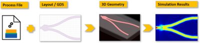
A foundry-compatible Y-splitter design simulated in Lumerical FDTD. Because the 3D geometry is generated by a combination of layout and the GF photonic process file, the simulation is compatible with GF fabrication process.
Photonic Verilog-A Circuit Simulation Enablement
Verilog-A is a popular modeling language for compact models of CMOS electronics circuit simulation. Rapid growth of CMOS-compatible SiPh is driving the development of photonic Verilog-A to support electronic-photonic co-simulation. However, due to a lack of standards, photonic Verilog-A developments have been fragmented among the ecosystem of players, leading to incompatibility between the models offered by different providers.
To overcome this barrier and the limits it imposes on designers, GF and Ansys came together to align their photonic Verilog-A models to be compatible (a first in the photonic industry). Users are now able to use models from Ansys and GF within the same circuit, thanks to jointly developed Verilog-A converter elements. Users can also use Lumerical CML Compiler to automate compact model generation for any custom components including those designed using the above-mentioned foundry-compatible design flow.
The figure below shows a schematic of a Mach-Zehnder interferometer, which is the basis for Mach-Zehnder modulators commonly used in optical transceivers. Converter elements have been added to allow a mixture of Ansys and GF photonic Verilog-A models. This new solution enables designers to take advantage of the extensive model libraries offered by Ansys and GF as well as the model generation capabilities of CML Compiler without the need to write their own models for the components that they design.
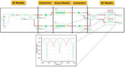
A Mach-Zehnder interferometer simulated with a combination of Ansys and GF photonic Verilog-A models. The converter elements enable the two types of models to talk to each other.
To get more familiar with Ansys’ photonic Verilog-A platform and compact modeling capabilities, explore the Verilog-A PAM4 transceiver example available in Ansys Lumerical’s application gallery and download a free 30-day trial of Lumerical CML Compiler.