Synopsys and Ansys power the future of innovation—connecting silicon to systems.
-
-
Access Free Student Software
Ansys empowers the next generation of engineers
Students get free access to world-class simulation software.
-
Connect with Ansys Now!
Design your future
Connect with Ansys to explore how simulation can power your next breakthrough.
Free Trials
Products & Services
Learn
About
Back
Products & Services
Back
Learn
Ansys empowers the next generation of engineers
Students get free access to world-class simulation software.
Back
About
Design your future
Connect with Ansys to explore how simulation can power your next breakthrough.
Free Trials
ANSYS ADVANTAGE MAGAZINE
DATE: 2020
Optimize High-Speed Serial Links for Crosstalk
By Dai Dai, Mixed-Signal IC Design Manager, NVIDIA Santa Clara, U.S.A.
Today’s system-on-chip (SoC) designs — regardless of application — just keep getting more complex. Specifically, high-speed chips become even more daunting when it comes to rooting out electromagnetic (EM) crosstalk and achieving an efficient power distribution network in a reasonable amount of time.
Consider, for example:
- Engineers in the automotive sector struggle with 80 GHz millimeter-wave radar chips with lots of on-die EM complexity. Crosstalk is of course an enormous concern on devices where safety is critical in the end product.
- In 5G cellular, engineers contend with an EM nightmare: lots of radios on the same die. Some teams have to simulate for 5,000 different frequency intermodulation products on a single 5G transceiver.
- Teams designing high-performance artificial intelligence chips like graphics processing units (GPUs) have to deal with multi-gigabit-per second input/output and the noise that can create.
- High-bandwidth memory and processor cores have to deal with complex multilayer silicon interposers that connect core and memory.
All these chips have two common denominators: high speed and high frequency.

NVIDIA’s NVLink technology road map shows throughput doubled over a two-year period. The tightly packed data links increase the risk of crosstalk.
When it comes to high-speed, chip-to-chip serial link design, we have been doubling throughput as fast as every two years, but we have to do it in the same area constraints. That means more tightly packed data links, which increases the risk of crosstalk.
Additionally, the latest GPU designs have widely employed interposers. Those interposers can cause additional crosstalk. If you don’t take into account the interposer, it will come back to bite you because you’ll have interposers on top of your inductors creating that coupling.
Also, because of large bump pitches (from 150 mm to 200 mm) and a limited number of bumps in a constrained area, it can be challenging when you want to separate noisy power domains, for instance the digital power and analog power domains. To do so, you need multiple power and ground bumps. When you have a large number of bumps, it’s hard to route power and ground cleanly. That worsens the crosstalk potential. You have to analyze what type of coupling is coming from power and ground for critical mass.
Knowledge Is Key
To improve signal integrity and power consumption, we need to be EM-aware. Because our team is constantly pushing the envelope on high-speed, high-frequency design, we’ve built an effective, efficient methodology to root out crosstalk issues in a way that does not bog down our schedule or tie down too many engineering resources.
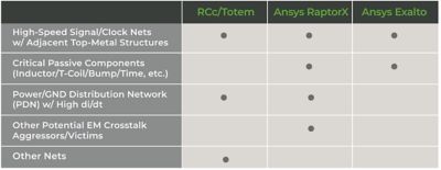
NVIDIA’S design methodology is hierarchical. We first classify everything into different categories, the most critical being high-speed signaling and clocking nets. We start with traditional resistance and capacitance extraction with coupling (RCc) extraction as part of a top-level simulation approach. In this initial exploration, we don’t need a lot of detail, but we do need fast turnaround time while we examine high-speed signals and clock nets and adjacent top-metal structures, as well as the power and ground distribution network. We turned to Ansys Totem, which does power grid weakness analysis, point-to-point checks, and a variety of early-stage static and dynamic IR and EM analyses that can highlight design weakness.
To perform additional analysis and optimization in the methodology, the team relied on Ansys RaptorX and Ansys Exalto to examine high-speed signal and clock nets; critical passives such as T-coils, inductors and bumps; power and ground; and other aggressors and victims that might cause EM crosstalk.
RaptorX is a post-layout RLCk extraction software solution that enables IC design engineers to accurately predict electromagnetic coupling effects during the signoff phase. It can capture unknown crosstalk among different blocks in the design hierarchy by extracting lumped-element parasitics and generating an accurate model for electrical, magnetic and substrate coupling. And Exalto integrates the above function with conventional RC extraction flow and makes it easier to use for designers.
Let’s look at some examples of how we implemented the methodology to explore crosstalk in various parts of our design and in turn optimized those designs based on the results.
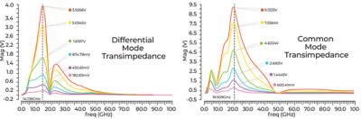
Plots show both differential- and common-mode crosstalk from a power delivery network to sensitive receiver signal nets vs. effective decoupling capacitors. Different colors in the figures means that different amounts of decaps were used in the configurations.
DataPath CrossTalk Analysis
The image below is a partial floorplan of a high-speed receiver in a recent NVIDIA GPU design. Because of area constraints and power-efficiency considerations, the inductors and T-coil have a limited keep-out region compared to conventional RF designs. You can’t afford a large region for these passive structures because you will have to space out all your high-speed circuitry. That in turn makes your overall design power-inefficient. To capture adjacent crosstalk effects, we used RaptorX to extract all critical nets and adjacent power/ground as n-port, with the partial layout including only the top, thick metal layers.
We extracted the entire area as a model. We put different ports in different locations, and ran S-parameter simulation as well as transient simulation to determine the crosstalk effects. Once we had the results, we reoptimized the layout and decoupling capacitator (decap) placements to minimize the crosstalk effect.
We wanted to try to reduce crosstalk effects at the frequency of interest by 2–10 times by putting decaps at correct locations; based on the transient wave forms at the bottom, we can see that the transient effects after optimization are reduced to 3 millivolts. It’s still there, but we minimized the impact based on our analysis.
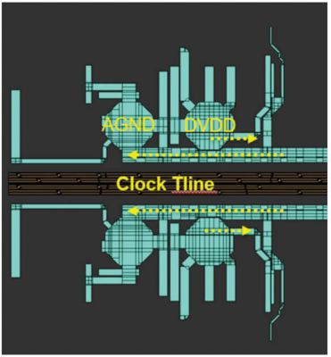
Power-Clock Line Challenges
Another big issue is crosstalk from power to high-speed clock lines. With SerDes (serializer/deserializer) design, often one phase-locked loop (PLL) will drive critical high-speed clocks to multiple different data lanes. This clock distribution can run for several millimeters depending on the application. Because of the area constraint, it’s hard to avoid noisy ground and power running in parallel with the clock lines. Even if you have proper shielding on the side of the clock, it’s not enough. You’ll still experience severe magnetic crosstalk from those power lines.
To capture the big picture, you have to put multiple data lanes together to include the entire clock distribution network. To do that, you need to extract more than 50 and sometimes as many as 100 ports. You can only really do this with RaptorX.
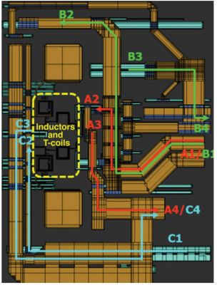
A partial floorplan of a high-speed receiver in an NVIDIA GPU design shows the limited keep-out region of on-chip passive components (inductors/T-coils).
When you extract the whole thing with power, ground and clock using RaptorX, you see much worse crosstalk jitter from the power and ground lines.
The two comparative plots allow NVIDIA to look at jitter. They show the same simulation at different locations. The yellow ones are based on RCc extraction.
Even after optimization, we’re seeing instantaneous jitter that is twice as bad as with RCc-only numbers. This effect is hard to eliminate completely, but with the proper setup and tool, you can predict it and include it in your jitter budget along with other random jitter (RJ) and deterministic jitter (DJ). If you ignore that, you’ll have a surprise in store for you when silicon comes back. We need this Ansys tool to ensure that we capture all effects from this sort of coupling.
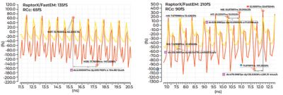
Two comparative plots allow NVIDIA to look at jitter. They show the same simulation at different locations. The yellow lines are based on RCc extraction.
How To Optimize Power Distribution
The figure below represents an optimization of a power delivery network (PDN) we performed using a combination of RaptorX and Exalto. Our analysis included both inductive top-metal layers as well as a bottom resistive lower via and metal. We put ports on all access points, including bumps, decoupling caps, current sinks and sources.
The decaps are optimized to reduce dependence on long, top-metal routings for high-frequency current delivery, while keeping high area efficiency. The current return path is planned carefully in parallel with the delivering path to minimize loop enclosure and reduce flux/routing inductance.
RaptorX enables NVIDIA to extract long clock routings plus the power delivery network over multiple lanes with a large
number of ports.
With this optimization, we were able to reduce the supply ripple induced by di/dt (the rate of change of the current) by 40%.
Efficiency At Scale
With advanced SerDes design, there are high-speed impairments that can’t be captured with simple RCc extraction as frequencies keep increasing. These impairments include EM crosstalk and di/dt-induced supply noise.
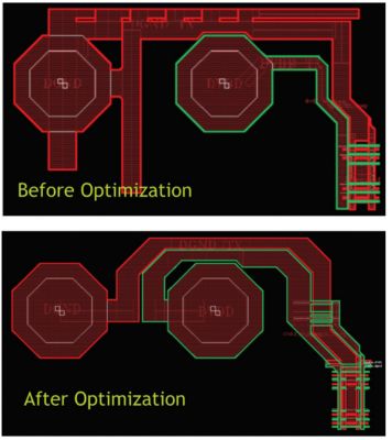
NVIDIA used Ansys RaptorX and Ansys Exalto to optimize a power delivery network.
We used a combination of RCc and EM tools to properly model all these. With RaptorX and Exalto, we were able to do a very large-scale extraction efficiently in a short time that allowed us to push the physical design to its limit while minimizing the associated risks. The end result was a power-efficient design.