Synopsys and Ansys power the future of innovation—connecting silicon to systems.
-
-
Access Free Student Software
Ansys empowers the next generation of engineers
Students get free access to world-class simulation software.
-
Connect with Ansys Now!
Design your future
Connect with Ansys to explore how simulation can power your next breakthrough.
Free Trials
Products & Services
Learn
About
Back
Products & Services
Back
Learn
Ansys empowers the next generation of engineers
Students get free access to world-class simulation software.
Back
About
Design your future
Connect with Ansys to explore how simulation can power your next breakthrough.
Free Trials
PRESS RELEASE
DATE: 03/25/2021
GUC and Ansys Expedite Advanced-IC Designs for Next-Generation Applications with State-of-the-Art Simulation Workflow
Ansys’ new workflow cuts model setup time from hours to minutes, runs simulations 2-3x faster, and expedites the integration of GUC die-to-die solution for ASICs
Key Highlights
- GUC engineers are using Ansys HFSS 3D Layout’s advanced simulation workflow to speed advanced integrated circuit (Advanced-IC) design
- Theworkflow helps GUC rapidly incorporate its die-to-die solution across CoWoS (Chip-on-Wafer-on-Substrate), InFO (Integrated Fan-Out) and interposer designs to create leading-edge artificial intelligence (AI), high-performance computing (HPC) and data center networking customer ASICs
PITTSBURGH, PA, March 25, 2021 – Global Unichip Corporation (GUC) is adopting a groundbreaking simulation workflow developed by Ansys (NASDAQ: ANSS) to accelerate Advanced-IC design. The workflow enables enhanced innovation across CoWoS, InFO and interposer designs, including GUC’s newly announced, silicon-proven GUC multi-die interLink (GLink) interface, which is essential for developing leading-edge AI, HPC and data center networking applications.
To maintain market leadership, GUC engineers must create, simulate and optimize Advanced-ICs with unprecedented speed, achieving first-pass design success and optimal device performance. However, major roadblocks stall the simulation process, especially in complex areas such as CoWoS, InFO design manipulation and device meshing.
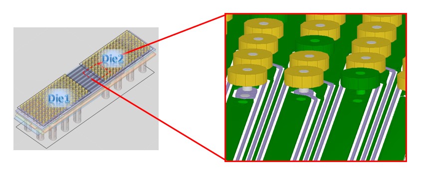
GUC delivers the industry-leading die-to-die interconnect solution for advanced customer ASICs.
Ansys HFSS 3D Layout’s workflow empowers GUC engineers to simulate faster and solve challenging geometries by incorporating several innovative tools, including ECADXplorer — a powerful new GDS editing platform that simplifies design manipulation to drive rapid simulation. Integrating cutting-edge meshing technologies coupled with Ansys’ industry-leading 3D HFSS solver, the workflow reduces simulation set-up time from hours to minutes. This helps GUC Advanced-IC designers efficiently extract S-parameter models of their devices with the highest fidelity. Additionally, it spurs the development of game-changing technologies such as GLink, which provides 6-10 times less power consumption than an alternative solution and occupies two times less silicon area.
“Advanced-IC package designs are highly sophisticated due to the ever-growing demand for increased functionality and lower power consumption within a smaller footprint. The strong momentum of GLink adoption by our AI, HPC and networking customers supports our commitment to building a wide IP portfolio and deepening GUC’s advanced packaging design expertise," said Igor Elkanovich, chief technology officer at GUC. “HFSS 3D Layout helps our engineering team decrease Advanced-IC design complexity, integrate heterogeneous chips and improve multi-chip performance to ensure customers receive new AI, HPC and Data Center Networking products much sooner.”
“Through this enhanced workflow, Ansys increases the productivity for GUC Advanced-IC designers by significantly simplifying the design process,” said Shane Emswiler, senior vice president at Ansys. “Leveraging HFSS 3D Layout, GUC engineers are swiftly creating fully parametric models, performing design studies of electronic packaging and exploring more design options than ever to evaluate tradeoffs prior to production — delivering considerable reductions in development time and expense.”
About GUC
Global Unichip Corporation (GUC) is the advanced ASIC leader, who provides the semiconductor industry with leading IC implementation and SoC manufacturing services, using advanced process and packaging technology. Based in Hsin-chu Taiwan, GUC has developed a global reputation with a presence in China, Europe, Japan, Korea and North America. GUC is publicly traded on the Taiwan Stock Exchange under the symbol 3443. For more information, visit https://www.guc-asic.com
About Ansys
If you've ever seen a rocket launch, flown on an airplane, driven a car, used a computer, touched a mobile device, crossed a bridge or put on wearable technology, chances are you've used a product where Ansys software played a critical role in its creation. Ansys is the global leader in engineering simulation. Through our strategy of Pervasive Engineering Simulation, we help the world's most innovative companies deliver radically better products to their customers. By offering the best and broadest portfolio of engineering simulation software, we help them solve the most complex design challenges and create products limited only by imagination. Founded in 1970, Ansys is headquartered south of Pittsburgh, Pennsylvania, U.S.A. Visit www.ansys.com for more information.
Ansys and any and all ANSYS, Inc. brand, product, service and feature names, logos and slogans are registered trademarks or trademarks of ANSYS, Inc. or its subsidiaries in the United States or other countries. All other brand, product, service and feature names or trademarks are the property of their respective owners.
ANSS–C