-
-
学生向け無料ソフトウェアにアクセス
Ansysは次世代の技術者を支援します
学生は、世界クラスのシミュレーションソフトウェアに無料でアクセスできます。
-
今すぐAnsysに接続!
未来をデザインする
Ansysに接続して、シミュレーションが次のブレークスルーにどのように貢献できるかを確認してください。
無料トライアル
製品およびサービス
リソースとトレーニング
当社について
Back
製品およびサービス
ANSYS BLOG
May 18, 2022
Simulating RF Desense and Electromagnetic Interference in Electronic Devices
It is a universal experience of modern life: You’re in an area of sufficient cellular signal, but the internet connection is degraded. A Bluetooth link is dropped even though the device battery is fully charged. The touchscreen of a device is unresponsive for no apparent reason.
Though the causes of such scenarios can be myriad, a common reason for degraded performance is when one part of an electronic device interferes with the performance of another part of the same device. It is easy to see how this can occur in modern electronics; it is common to include Wi-Fi, Bluetooth, Global Navigation Satellite System (GNSS), and cellular functions on devices that in another era would remain as separate devices. Further, devices’ wired cable connections are expected to support high data rates and carry increasingly higher power. The clock frequency of data rate transmission and its harmonics may extend into the same band as radio frequency (RF) receivers in the device. Manufacturers that include a cable connection have little control over the behavior of another device that users may connect to their own device.
Device manufacturers and integrators of third-party components are tasked with the challenge of maintaining self-compatibility of electronic systems. The concern is that electromagnetic interference (EMI) from printed circuit board (PCB) traces or cables on or near the product will de-sensitize (desense) the performance of the device’s RF systems.
Often, a challenge in modeling desense and EMI in electronics is the complexity of the geometry of the electronic device itself. The complexity can be seen in the wide range of length scales in electronics: cables may be meters long while cable braid conductors are sub-millimeter. On a device, the traces and antenna elements are equally small. The enclosure and outer dimensions of the cable are represented via mechanical computer-aided design (CAD) files; however, there may not be mechanical CAD representations of the interior of cables, the braids, or electronic components.
Another challenge is the multidisciplinary nature of the problem. The desense and EMI issues require input from the RF group who is designing the antennas and RF components. The enclosure and device structures are designed and maintained by a mechanical design team. Passive shielding components may have been specified from an electromagnetic compatibility (EMC) team, but they are often implemented and designed by the mechanical group. Further, there may be a wiring group that is responsible for the data cables, power cables, and their associated shields and connectors. The details of the signals on data lines and emissions on power lines are specified via circuit models and maintained by signal and power integrity (SI/PI) engineers.
How to Approach Multidisciplinary Model Complexity
Ansys EMA3D Cable addresses both the model complexity and multidisciplinary nature of the EMI and desense problem. Let's take a modern approach to considering complex product design for self-compatibility.
The figure below shows the 3D geometry of a typical electronic device. There are connectors, cables with shields around the conductors, an enclosure, antennas, and PCBs with traces. The 3D geometry for structures is imported from mechanical CAD, while some PCB definitions are specified in electronic CAD and merged into the same model. The path of the cable may be present in mechanical CAD, but generally the interior conductors and details of the shield are omitted. Instead, they are represented in the simulation using a hybridized co-simulation with a modified multiconductor transmission line (MTL) solver in EMA3D Cable. The cable representation in the product allows users to specify the cable by the 2D cross section, while the path of the cable is defined by a line in 3D. The combination of 2D cross section specification of conductors and 3D specification of the path greatly reduces the time to define a cable in a way that captures the essential electromagnetic elements.
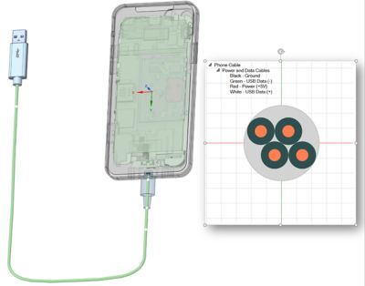
A 3D description of a cell phone. The cable has conductors and a shield, and the phone consists of a case and internal electronics. The electronics include printed circuit board traces, a liquid crystal display screen, optics, and antennas.
Once the 3D structures and cable harness have been specified, it is important that signals on the components, traces, antenna ports, and cable conductors match real product performance. In most cases, the best description for power and signal operation is through transient circuit models. EMA3D Cable includes the Nexxim circuit solver, allowing engineers to take existing electronic designs and apply them to cable and 3D components. This saves time by allowing for circuit reuse.
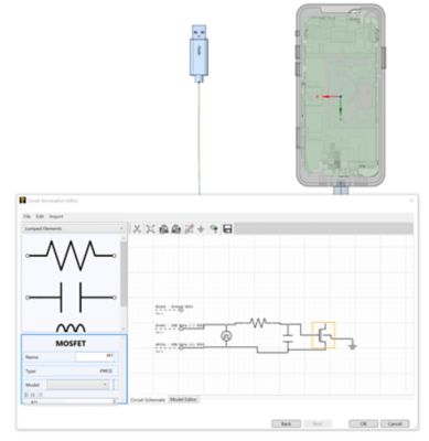
Time domain simulation in 3D, multiconductor transmission line (MTL) simulation, and transient circuits are co-simulated timestep by timestep to facilitate analysis of the interaction between data communication circuits and antenna-connected radio frequency (RF) ports.
It is important that engineers studying EMI and desense are able to create accurate models of their RF systems. Through a combination of the Nexxim transient circuit solver and the 3D solver, details of the performance of RF systems can be analyzed in EMA3D Cable. In the next figure, the geometric details of the Wi-Fi antenna are shown.
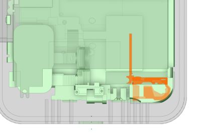
The Wi-Fi antenna is highlighted in orange. The antenna is connected to the “victim” receiver in the interference analysis.
Engineers may wish to analyze RF system performance to ensure that it is properly represented in the model. EMA3D Cable allows you to quickly specify the antenna port to determine the return loss versus frequency using scattering parameter (S-parameter) analysis. Ports are defined with a single click on the location in 3D. EMA3D Cable automatically computes the S11 for return loss, as shown in the next figure. The plot shows resonances at the primary Wi-Fi operational frequencies.
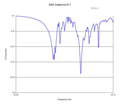
A scattering parameter (S-parameter) plot of Wi-Fi antenna return loss (S11) versus frequency. The return loss is minimized at the two primary WiFi frequencies of interest.
Next, the coupling between the antenna and one of the cable conductors is simulated by EMA3D Cable. The method for specifying the port on the cable is like that described above for the antenna. With both ports defined, EMA3D Cable calculates the S12 for coupling between the two as a function of frequency. The next plot shows the coupling from the cable to the antenna port. The simulation proceeds as a hybrid co-simulation of the 3D full-wave solver, the cable solver, and the Nexxim transient circuit.
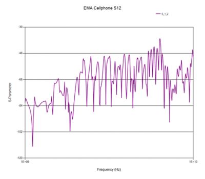
An S-parameter plot of the coupling between the antenna and a conductor within the phone cable (S12) .
In addition to calculation of coupling, the 3D solver reveals the fields and currents at all locations in space. In the following figure, the electric field normal to a slice through the phone and cable is plotted at a specific point in time.
False-color plot showing the magnitude of the electric field normal to a plane that slices through the phone and cable. A conductor within the cable is initially excited by a short voltage pulse.
Intra-system RF interference in an electronic device is a significant challenge for design engineers that must be addressed in an increasing number of products. We have shown a workflow that allows desense and EMI engineers to pull design and circuit descriptions from a wide range of data formats and synthesize them into a single simulation. We show how EMA3D Cable performs a self-consistent simulation using a 3D full-wave solver, a cable solver, and a transient circuit solver. Analysis of antenna performance, the coupling of interference, and unintentional emissions may be calculated with a streamlined workflow. This simulation technology allows electronics designers to predict potential interference and compliance issues in early program phases when applying mitigations are less costly and impactful to development schedules.
Learn more about Ansys EMA3D Cable.