-
-
Access Free Student Software
Ansys empowers the next generation of engineers
Students get free access to world-class simulation software.
-
Connect with Ansys Now!
Design your future
Connect with Ansys to explore how simulation can power your next breakthrough.
Countries & Regions
Free Trials
Products & Services
Learn
About
Back
Products & Services
Back
Learn
Ansys empowers the next generation of engineers
Students get free access to world-class simulation software.
Back
About
Design your future
Connect with Ansys to explore how simulation can power your next breakthrough.
Free Trials
ANSYS BLOG
March 26, 2021
PCB Design Rules for Electromagnetic Compatibility
When it comes to electromagnetic interference (EMI) and printed circuit boards (PCBs), rules are not meant to be broken. Following some simple guidelines for electromagnetic compatibility when designing PCBs will save time and costs. Simulation software can help.
All high-speed signals on a PCB should be referenced to a solid plane. A current flowing in any trace on a PCB must complete the entire circuit loop and come back to the source (yellow arrow in figure 1a) through the reference plane. The return current will always choose the path of least “impedance” and will form the smallest loop with respect to the incident current path to minimize loop inductance (refer figure 1b):
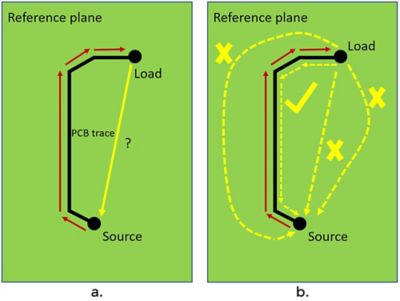
Figure 1: Current flowing through a PCB trace and return path of least inductance
If the signal reference is not accounted for correctly, it may lead to potential EMI issues in the product. Let’s look at some important signal reference related design guidelines. Also, we will look at how Ansys SIwave, through its built-in EMI Scanner, enables an automatic and customizable signal reference rules check of PCBs to identify areas of potential issues.
Rule 1: Net Changing Reference
Usually, high-speed signal traces change multiple layers through vias on the PCB. While doing this, one tends to forget how the return current will flow back between the two layers. This is illustrated in figure 2a where due to the proximity, the trace references to plane 1 when on top layer and to plane 2 when it goes to the bottom layer through the via. Because the return current path is broken, it can lead to unintended EMI issues and unwanted radiation in the via region.
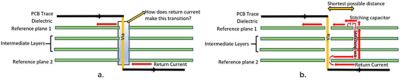
Figure 2: Signal trace changing reference
If the reference change is unavoidable, the two reference planes must be connected through stitching capacitors and/or vias. These must be placed as close as possible to the signal transition region, allowing the return current to flow forming the shortest possible loop, as shown in figure 2b.
Rule 2: Net Near Edge of Reference
When the trace is not routed near the edge of the reference plane, the electric field couples well from the trace to the reference plane and is well contained within the PCB. Figure 3a shows an example of a trace with its reference plane. On the other hand, if the trace is routed near to the edge of the reference plane (figure 3b), the E-field lines are no longer contained and can leak outside the intended PCB plane.
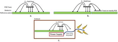
Figure 3: E - field comparison for trace routed away from and close to edge of reference
These leaked E-field lines can cause unintended coupling to a trace on an adjacent board within a system. Also, if these electric fields couple to a cable exiting the system (figure 3c), it can cause unintended radiation and radiated emission issues.
Rule 3: Net Crossing Split
Sometimes, PCB designers may introduce a split in the high-speed trace reference plane. Figure 4a shows a split in the reference plane that forces the return current to go around the split, meaning a longer path, higher loop inductance and EMI issues. A split is not recommended, but in cases where it is unavoidable, having a stitching capacitor across the split as shown in figure 4b provides the high frequency return current path without much deviation across the split. These capacitors should be placed as close as possible to the net crossing.
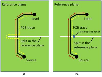
Figure 4: Return current path in the presence of a split in the reference plane
Let’s use this rule in a SIwave EMI Scanner simulation example to illustrate the impact of the split.
Net Crossing Split Example: Simulation and Relation to Actual Test Requirement
In the PCB example in figure 5, a net crossing split rule in EMI Scanner identifies two points at which the net SPI1_SCK crosses two different splits in the reference plane and reports them as violations.
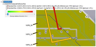
Figure 5: Violations reported by EMI Scanner for SPI1_SCK
For analysis purposes, two pairs of capacitors (value 0.1μF) are created (two numbers each across the splits), shown in figure 6:

Figure 6: Stitching capacitors created across the splits
We run the near field analysis in SIwave before and after introducing the capacitors. In the area where the net SPI1_SCK crosses the split, the result is as shown in figures 7a/7b for the before condition, and in figures 7c/7d for the after condition.

Figure 7: Near field @ 828.46 MHz and 162.45 MHz before and after introduction of capacitors
The violations in the EMI scanner go away, and the near fields plots show a reduction in the levels.
Usually, an automotive component is tested against CISPR 25 radiated emissions requirements at distance of 1 meter. Figure 8 shows a comparative analysis of simulated far field from this PCB at a - meter distance in the frequency range 30 MHz ‒1 GHz. Note that the inclusion of stitching capacitors brings down the emission levels by 5 ‒ 10 dB. If we consider two limits from CISPR 25 for simplified analysis, we see class 5 peak limits of 28 dBμV/m @ 41 ‒ 88 MHz (TV Band I) and 35 dBμV/m @ 142 ‒ 175 MHz (VHF). The PCB shows non-compliance in these frequency ranges without the stitching capacitors.
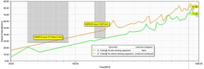
Figure 8: A 1-meter radiated emissions comparison
Having looked at the signal reference related PCB design guidelines, namely net changing reference, net near edge of reference and net crossing split, it is clear that signal reference has a vital role to play in being able to avoid EMI issues at the PCB level and subsequently at the product level.
SIwave’s EMI Scanner simulations on PCB level enable early identification of such EMI issues, which helps the PCB designer make design changes that can then be re-simulated to gain confidence before it is passed on for further component- and system-level simulations or physical testing.
To learn more on how to use SIwave’s EMI Scanner check out the video below and other videos on our SIwave Youtube channel.