Synopsys and Ansys power the future of innovation—connecting silicon to systems.
-
-
Access Free Student Software
Ansys empowers the next generation of engineers
Students get free access to world-class simulation software.
-
Connect with Ansys Now!
Design your future
Connect with Ansys to explore how simulation can power your next breakthrough.
Free Trials
Products & Services
Learn
About
Back
Products & Services
Back
Learn
Ansys empowers the next generation of engineers
Students get free access to world-class simulation software.
Back
About
Design your future
Connect with Ansys to explore how simulation can power your next breakthrough.
Free Trials

Chances are good at this moment that there’s at least one device close to you that uses miniaturized optics. If you find yourself checking your daily steps or your vitals or even snapping a selfie with your bestie, you probably have miniature devices to thank.
The miniaturization of optics and photonics is part of a continuing industry trend toward the creation of smaller, lighter, more efficient devices at the pace of modern innovation.
“Miniaturization refers to shrinking the sizes of optical components and systems while ensuring their performance remains the same, if not better,” says Amrita Pati, senior engineer, applications engineering at Ansys, part of Synopsys. “This often involves new materials, manufacturing techniques, and even rethinking fundamental physical schemes.”
In the miniaturization of optical components, including lenses, sensors, and circuits, optical engineers are unlocking new possibilities in many fields, from healthcare to telecommunications, to do amazing things.
Small Trends Yield Big Performance
Advancements in miniaturization are paving the way for even smaller, more powerful devices across industries. Perhaps the biggest development is the metalens, an ultrathin lens engineered using nanostructures. These structures are materials with at least one dimension on the nanoscale (an extremely small structure, significantly smaller than a single strand of human hair).
“Metalenses are transforming optics by replacing bulky, curved glass with ultrathin, flat surfaces that use nanostructures to manipulate light,” says Pati. “This shift not only advances miniaturization but also unlocks possibilities for creating lightweight, compact devices without compromising optical performance.”
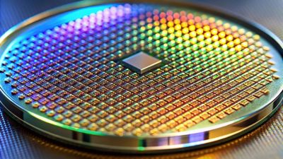
From wafer to breakthrough: Precision simulation enables the design and manufacturing of next-generation semiconductor devices.
Despite their nearly incomprehensible size, metalenses deliver superior optical performance when compared with traditional glass optics. For this reason, these miniature lenses are poised to transform imaging and sensing technologies in consumer electronics. They are often found in autonomous vehicles, medical devices, and surveillance systems, as well as display and imaging systems.
Another big trend is the use of photonic integrated circuits (PICs) created by combining optical components into a single chip. These devices are finding their way into more complex sensing applications, as they incorporate multiple photonic functions in an incredibly small form factor.
How do PICs translate in everyday life? They’re quickly replacing bulky optical assemblies to enable faster data transmission in telecommunications and improve the accuracy of lidar-based sensing systems used in autonomous vehicles. PICs can also be found in wearable health monitors and environmental sensors, where they are used to deliver real-time insights in a portable format.
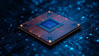
Powering next-generation innovation: High-fidelity simulation is at the heart of advanced electronics and photonic systems.
Taking a Nano-Sized Approach to Integration
Another benefit of miniaturization is that it facilitates integration.
In optics and photonics, integration is the process of combining optical and photonic components into one cohesive system. In doing so, engineers can reduce system complexity and enhance the reliability of devices — a key factor in the development of augmented reality (AR) and virtual reality (VR) applications, where miniaturized optics and displays enable lighter, more comfortable headsets.

Design immersive extended reality (XR) experiences with Ansys Optics software, where advanced optical simulation brings virtual worlds into sharp, comfortable, and realistic focus.
“Through the convergence of integration and miniaturization in optics, we’re witnessing a shift toward highly efficient, scalable systems that maintain the exceptional performance of traditional optics while reducing size and complexity,” says Pati.
However, integration at the nanoscale has led to some significant challenges and several innovations helpful to overcoming them:
- Advanced materials, such as metasurfaces and photonic crystals, play a crucial role during integration due to their ability to enable unique optical properties. Access to these and other materials enables the more effective manipulation of light to further enhance performance in a complex form factor.
- Freeform optics offers additional degrees of freedom to design optical components, ultimately enabling more precise control over light. Freeform optics is a departure from traditional lenses, as irregular surfaces are used to eliminate optical aberrations, thus requiring fewer corrective components.
- Wafer-level manufacturing facilitates the simultaneous production of multiple components on a single wafer. This method supports the successful integration of optical systems in compact spaces, reducing alignment errors in the process. It also facilitates batch processing to further scale production in terms of both time and cost.
- Photonic integration involves the embedding of multiple photonic components into a single chip. This approach enables optical engineers to enhance performance while reducing size, power consumption, and manufacturing complexity, particularly in the optimization of integrated circuits, ever mindful of requirements.
- Simulation helps engineers make predictions in support of these innovations and techniques through the modeling behavior of components under various conditions, thus mitigating any issues ahead of time. Virtual testing ensures their successful integration and ultimately their performance, even as components shrink in size.
Managing Challenges in Miniature With Simulation
Of course, achieving seamless integration is prone to its own challenges, including the precise alignment of optical elements and the management of heat dissipation in densely packed systems. And optical engineers are turning to simulation to address them all.
Simulation tools enable engineers to model and optimize integrated system performance before committing to building a single physical prototype. The tools can be used to help identify and optimize component alignment. They can also predict how a specific material or materials will behave under real-world conditions.
Ansys, part of Synopsys, provides a suite of tools specifically designed to address the challenges of miniaturization and integration in optics and photonics, including:
- Ansys Lumerical FDTD software specializes in simulating the behavior of light at the nanoscale, making it ideal for designing subwavelength components, such as diffraction gratings and meta-optics.
- Ansys Zemax OpticStudio software focuses on ray optics, enabling engineers to model larger optical systems, including lenses and beam splitters, with precision.
- Ansys Speos software enables human vision analysis and scene rendering, ensuring that the final optical system performs well under real-world conditions.
The seamless integration of these tools makes it possible for engineers to address multiscale challenges quickly and efficiently, from nanoscale component design to system-level performance analysis.
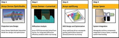
An end-to-end augmented reality (AR) optical design workflow: projection lens design in Ansys Zemax OpticStudio optical system design and analysis software, diffraction analysis with Ansys Lumerical FDTD advanced 3D electromagnetic FDTD simulation software, design of experiments (DOE) optimization in Ansys optiSLang process integration and design optimization software, and full system integration and validation in Ansys Speos CAD integrated optical and lighting simulation software
“With Ansys tools, engineers can tackle multiscale physics, from numerical simulations of nanostructures with Lumerical software to larger system designs using Zemax software and finally analyzing user experience through human vision simulations in Speos software,” says Pati.
Miniaturization Is Necessary
Today, miniaturization is not just a convenience but a necessity for staying competitive in an ever-evolving technological landscape. As industries increasingly prioritize performance, portability, and energy efficiency in our devices, the miniaturization of optical and photonic systems will be crucial to their success.
To learn more about optical miniaturization and how Ansys can help support those efforts, make sure to check out the e-book detailing Ansys miniaturization solutions. Also, explore the Ansys Optics 2026 Webinar to Workshop Series.
Just for you. We have some additional resources you may enjoy.
Get the E-book
To learn more about optical miniaturization and how Ansys can help support those efforts, make sure to check out the e-book detailing Ansys miniaturization solutions.


The Advantage Blog
The Ansys Advantage blog, featuring contributions from Ansys and other technology experts, keeps you updated on how Ansys simulation is powering innovation that drives human advancement.