-
-
Access Free Student Software
Ansys empowers the next generation of engineers
Students get free access to world-class simulation software.
-
Connect with Ansys Now!
Design your future
Connect with Ansys to explore how simulation can power your next breakthrough.
Free Trials
Products & Services
Learn
About
Back
Products & Services
Back
Learn
Ansys empowers the next generation of engineers
Students get free access to world-class simulation software.
Back
About
Design your future
Connect with Ansys to explore how simulation can power your next breakthrough.
Free Trials
ANSYS BLOG
June 8, 2023
Exploring the Journey of Light, from Fiber to Chip Coupling
In the realm of high-speed communication and data processing, fiber-optic technology has become indispensable. The ability to transmit vast amounts of data quickly and efficiently has led to the widespread adoption of fiber-optic networks. To leverage the benefits of fiber optics at the chip level, light traveling in fibers needs to be efficiently coupled in and out of chips. Coupling electromagnetic light waves from a fiber to a chip is an intricate process.
Let’s take a look at the signal’s journey from the light wave’s perspective. Light in optical fibers is typically guided by total internal reflection. When a light wave travels through a fiber, it undergoes multiple reflections at the core-cladding interface, allowing it to propagate along the fiber's length. The wave is characterized by its electric field (E-field) and magnetic field (H-field) components, which oscillate perpendicular to each other and to the direction of propagation. Now imagine the captivating journey, in which light waves traverse the fiber and carry information and energy, only to be embraced by the chip's optical waveguide — unlocking its boundless potential.

As we approach the fiber-to-chip interface, a remarkable interplay of mechanisms and physics unfolds. Geometric matching is the first act in this grand performance. It is essential that the dimensions of the fiber's core align precisely with the waveguide on the chip. This alignment ensures optimal overlap of the optical fields, setting the stage for efficient coupling.
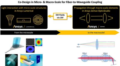
To enhance our coupling endeavor, designers typically use additional elements. Meticulously designed tapered structures guide the light wave through a gradual change in the waveguide's dimensions. This smooth transition ensures a seamless coupling process, enabling the light wave to gracefully navigate the landscape of the chip. The introduction of lenses can further enhance performance by focusing the light onto the waveguide with precision.
Fiber to Chip Coupling Efficiency Challenges
There are several factors that can influence overall coupling efficiency. Mode mismatch poses a significant hurdle. It occurs when the patterns of the light wave in the fiber and the waveguide do not align. To overcome this, designers employ mode converters and filters, which align the respective modes.
Alignment tolerances pose another challenge. Even the slightest misalignment between the fiber and the waveguide can introduce losses and diminish coupling efficiency. Factors such as thermal effects and mechanical constraints further accentuate the need for precise alignment during the packaging process.
Polarization dependency adds another layer of complexity. Light waves possess distinct polarization states, and some coupling methods are sensitive to these states. To address polarization-dependent losses, careful management of polarization sensitivity becomes crucial, allowing for consistent and reliable coupling.
Additionally, material absorption and scattering can diminish the efficiency of optical coupling. By selecting suitable materials and ensuring high-quality fabrication, we can minimize these losses. Variations in fabrication, such as deviations in waveguide dimensions or surface roughness, demand meticulous control and precision to mitigate additional losses.
In conclusion, the coupling of light from a fiber to a chip is an intricate interplay of mechanisms and physics. Designers strive to achieve efficient and reliable coupling through geometric matching; the introduction of tapered structures and lenses; and the management of challenges such as mode mismatch, alignment tolerances, polarization dependency, material interactions, and fabrication variations. It is through this coupling process that we unlock the potential of the chip, harnessing the power of light for a multitude of applications.
Check out our webinar “Simulation and Designs for Optical Coupling in PICs & Co-packaged Optics” for an in-depth presentation on optical coupling simulation methodologies and multiscale simulation workflows, as well as to see how designers can leverage a combination of Ansys Lumerical FDTD, Ansys Lumerical MODE, and Ansys Zemax OpticStudio for the design and optimization of chip-to-chip and chip-to-fiber couplers. See additional relevant resources to get started with the design of various optical coupling interfaces: