Synopsys and Ansys power the future of innovation—connecting silicon to systems.
-
-
학생용 무료 소프트웨어에 액세스하기
차세대 엔지니어에게 힘을 실어주는 Ansys
학생들은 세계적 수준의 시뮬레이션 소프트웨어를 무료로 이용할 수 있습니다.
-
지금 바로 Ansys에 연결하십시오!
미래를 설계하기
시뮬레이션이 다음 혁신을 어떻게 지원할 수 있는지 알아보려면 Ansys와 연결하십시오.
무료 트라이얼
제품 및 서비스
학습하기
회사 정보
Back
제품 및 서비스

In the early days of data centers, calculation speed was the bottleneck, and faster chips were the answer.
Today, things look very different. With the rapid rise of artificial intelligence (AI), hyperscale computing, and advanced networking, raw compute performance still matters — but it’s no longer the only bottleneck.
The issue is intensifying further as data rates double generation after generation, now reaching 448G. Emerging architectures, including co-packaged optics, chiplets, and ultra-high-density interconnects, are pushing signal speeds, power densities, and thermal loads beyond the limits of legacy materials, making it harder to meet insertion loss and reliability targets.
Consider high-speed electronics like AI servers or networking gear, where signals travel as electrical pulses through tiny metal traces on circuit boards or chips. The insulating materials around those traces — called interlayer dielectrics (ILDs) — play a crucial role. They prevent unwanted current flow, shape electric fields, and provide mechanical and thermal structure. The problem is that these materials were originally designed for slower speeds and less demanding radio frequency (RF) and high-speed digital applications.
Here’s why that matters. As frequency rises to 224G, dielectric insulators start absorbing more energy than at lower data rates, leading to weaker, distorted signals and increased heat. At 448G, the issue becomes even more pronounced: dielectric loss turns into a major limiting factor, directly affecting signal integrity, power consumption, thermal load, and the maximum achievable data rate.
In other words, physics is now the bottleneck. To move forward, the industry likely needs an entirely new class of materials.
Bridging the Gap Between Materials and System Performance
Thintronics, an interconnect technology startup, is tackling this challenge head-on by rethinking how ILDs are designed and manufactured — all the way down to the molecular level.
To ensure that its ILDs will solve multiphysics challenges in the real world, not just the lab, Thintronics integrated expertise from multiple domains: semiconductor engineering, materials science, chemistry, and advanced packaging. Because simulation links material properties directly to system-level performance, it became the bridge, enabling experts in each discipline to work from the same model from the beginning.
With access to the software through the Ansys Startup Program, Thintronics was able to get up and running significantly faster than it would have independently. Support from SimuTech, an Ansys Apex Channel Partner, helped them scale simulation capabilities, resulting in a complex project for predicting the reliability of modern multichip packages.
Delivering a First-of-Its-Kind Solution

Designing materials that solve real system bottlenecks isn’t straightforward. You have to strike a balance: understand what properties improve performance while also meeting the demands of real computing environments.
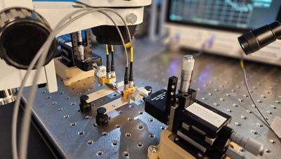
Probe station setup for mmW measurements
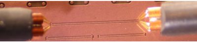
mmW transmission line structure and probes
Thintronics achieved these complementary goals by pairing bottom-up materials science research with top-down architecture understanding. In other words, while some Thintronics researchers focused on molecular or chemical structure, dielectric properties, thermal properties, and mechanical strength, others looked at the performance requirements that materials and components must meet.
Together, they produced the Thintronics-on-Substrate (TOS) platform, the first high-performance, ultra-low-loss substrate dielectric film made in the U.S.
Designed for today’s AI and high-performance computing (HPC) workload, the TOS platform delivers faster, more reliable, and more energy-efficient high-speed data movement across the entire interconnect path, not just one layer. Compared with conventional insulator materials, substrates manufactured with the TOS platform enable:
- 30% to 50% improved insertion loss at 224G/448G
- Up to a 42% reduction in serializer/deserializer (SerDes) circuit power consumption
- Up to a 17% reduction in AI data center energy consumption
- Ultra-low dielectric constant materials for more reliable interconnects and lower parasitic effects
HFSS Capabilities Help Push High-Speed Boundaries
Since joining the Ansys Startup Program in 2023, Thintronics has used Ansys products to help ensure that its customers’ boundary-pushing, high-speed SerDes packages perform in the real world. This is no easy task considering that these packages are “unforgiving of even the smallest discontinuity,” according to Lead Electrical Engineer Ehsan Foroozanfard.
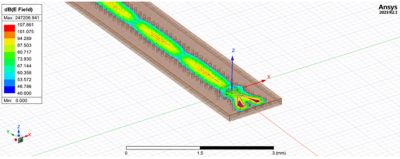
Simulated differential channel in HFSS software, showing the transition from grounded coplanar waveguide (GCPW) to stripline, representing a typical interconnect architecture used in advanced packaging for high-speed transmit and receive signal paths
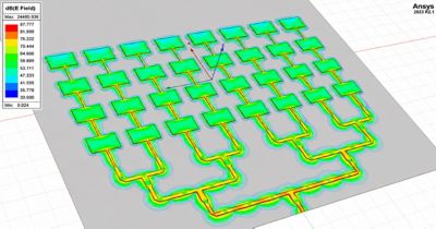
HFSS simulation of an E-field and surface current distribution of an 8-element antenna array with an integrated power splitter on a substrate, designed for 77 GHz radar applications
“A geometry that would be completely harmless at 10 Gbps becomes a serious signal integrity liability at 448 Gbps,” he says.
To better understand performance at higher frequencies, Thintronics used Ansys HFSS high-frequency electromagnetic simulation software to see how its designs would behave in real-world conditions. This helped the team quickly refine both materials and interconnects together, avoid potential signal issues early, and reduce development risk. The approach was also validated by closely matching simulation results with real-world measurements up to 67 GHz, providing what Foroozanfard calls a “stellar” correlation.
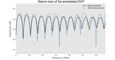
Return loss of the transmission, simulation and measurement over the frequency
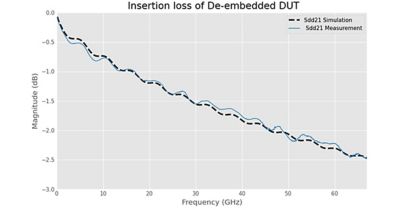
Insertion loss of the transmission, simulation and measurement over the frequency
“That level of agreement gave us — and our stakeholders — very high confidence that the simulation models were truly predictive, not just illustrative. It meant that design decisions made in simulation would hold up in hardware, which is the ultimate goal of any simulation-driven design flow,” he says.
Speed Without Sacrificing Accuracy
HFSS wasn’t the only tool in play. Thintronics also used several other Ansys solutions to round out its workflow.
Beyond electrical performance, Thintronics leverages mechanical simulation to understand how materials behave under real-world conditions across chip, package, and printed circuit board (PCB) scales. By modeling temperature-dependent properties and stress-strain behavior, the team ensures that advanced packaging designs meet both performance and durability requirements.
Mechanical modeling is tightly integrated with materials development at Thintronics. By feeding real characterization data — such as modulus and coefficient of thermal expansion — into simulations, engineers can more accurately predict reliability and guide material design decisions early in the development cycle.
For example, Ansys Mechanical structural finite element analysis software enabled the simultaneous simulation of high-speed SerDes channels across these scales, which helped engineers understand how materials behave at every level of the system. Used alongside Ansys Slwave PCB and package electromagnetics simulation software and the Ansys 3D Layout feature, engineers could simulate in detail just the important part of the package — and not waste time on a full-fidelity simulation of the entire package. This gave engineers the ideal balance of speed and precision: fast design iteration without sacrificing accuracy.
Test Hundreds of Variations — or Build One Prototype?
Thintronics’ experience highlights just how powerful simulation can be when designing next-generation interconnects. Validating performance through physical testing alone would be incredibly difficult — if not impractical. Simulation makes it possible.
By evaluating signal integrity, material behavior, and reliability early in the design cycle, simulation reduces reliance on costly, time-consuming prototypes that can run tens of thousands of dollars and take months. In that same time frame, engineers can test hundreds of design variations virtually.
Simulation also helps identify weak points where mechanical stresses may cause failures. For instance, differences in material expansion during thermal cycles can crack microvias, which are critical vertical connections in dense interconnects. Modeling thermal expansion and stress distribution enables engineers to pinpoint hotspots, estimate failure risk, and refine designs before fabrication.
Because high-speed systems involve tightly linked physical effects, multiphysics simulation also enables teams to optimize electrical performance, thermal behavior, and structural reliability at the same time — avoiding issues like signal loss or vibration that might otherwise be missed.
A Faster Path Forward
Thintronics is tackling one of the toughest challenges in semiconductor packaging today, and simulation sits at the heart of its approach.
By enabling Thintronics to close the loop among material characterization, simulation, and validation — and providing a more complete understanding of how designs will behave in the real world — simulation is accelerating the company’s path from concept to implementation.
We can’t go back to the early days of computing and, realistically, no one would want to. Computing systems will continue to push the boundaries of speed and complexity. And the kind of simulation-driven approach that Thintronics has taken will be essential in enabling faster, more efficient, and more reliable electronics.
See how the Ansys Startup Program can help you turn complex, high-speed design challenges into real-world solutions.

Just for you. We have some additional resources you may enjoy.
“It meant that design decisions made in simulation would hold up in hardware, which is the ultimate goal of any simulation-driven design flow.”
— Ehsan Foroozanfard, lead electrical engineer, Thintronics


The Advantage Blog
The Ansys Advantage blog, featuring contributions from Ansys and other technology experts, keeps you updated on how Ansys simulation is powering innovation that drives human advancement.
시작하기
엔지니어링 과제에 직면하고 있다면우리 팀이 도와드리겠습니다. 풍부한 경험과 혁신에 대한 헌신을 가지고 있는 우리에게 연락해 주십시오. 협력을 통해 엔지니어링 문제를 성장과 성공의 기회로 바꾸십시오. 지금 문의하기