-
-
Software gratuito per studenti
Ansys potenzia la nuova generazione di ingegneri
Gli studenti hanno accesso gratuito a software di simulazione di livello mondiale.
-
Connettiti subito con Ansys!
Progetta il tuo futuro
Connettiti a Ansys per scoprire come la simulazione può potenziare la tua prossima innovazione.
Paesi e regioni
Customer Center
Supporto
Partner Community
Contatta l'ufficio vendite
Per Stati Uniti e Canada
Accedi
Prove Gratuite
Prodotti & Servizi
Scopri
Chi Siamo
Back
Prodotti & Servizi
Back
Scopri
Ansys potenzia la nuova generazione di ingegneri
Gli studenti hanno accesso gratuito a software di simulazione di livello mondiale.
Back
Chi Siamo
Progetta il tuo futuro
Connettiti a Ansys per scoprire come la simulazione può potenziare la tua prossima innovazione.
Customer Center
Supporto
Partner Community
Contatta l'ufficio vendite
Per Stati Uniti e Canada
Accedi
Prove Gratuite
ANSYS BLOG
February 29, 2024
What is Co-packaged Optics?
Co-packaged optics (CPO) is an approach that aims to address growing challenges around bandwidth density, communication latency, copper reach, and power efficiency in today’s data-hungry networks by bringing key elements needed for communication closer together — namely optics and electronics.
Today, the industry employs different terms such as optical input/output (OIO) and CPO, leading to some confusion especially as near-package optics (NPOs) are often incorrectly labeled as CPOs. To clarify, the broader trend for CPOs is the same as with OIOs, in which there is a shift toward chiplet-based technology with optics integrated in a three-dimensional integrated circuit (3D-IC) package.
Pluggable Optical Transceivers and Beyond
In a world with an insatiable appetite for data that’s driven by high-resolution video streaming, virtual reality, Internet of Things (IoT), high-performance computing (HPC), and artificial intelligence and machine learning (AI/ML), networks and data centers globally face heightened demands for increased bandwidth, reduced latency, and lower power consumption.
Optics, initially only dominant in long-haul communications, has long penetrated data centers at shorter distances as well, with pluggable optical transceivers enhancing bandwidth density to and within racks. While these transceivers have evolved from 100G to 400G, 800G, and 1.6T, their power consumption becomes detrimental at higher speeds, especially in data-intensive applications like AI. Moreover, bandwidth scalability and form factors of “pluggables” pose limitations for future capacities like 6.4T and 12.8T.
To address these challenges, the industry is actively investing in CPOs and OIOs, heralding the next generation of solutions tailored to meet the evolving needs of emerging applications and future high-capacity network requirements. Collaborations among consortia, multi-supplier agreements, and standard agencies such as the Institute of Electrical and Electronics Engineers (IEEE) and the Optical Internetworking Forum (OIF) aim to create alignment on the specifications of CPO solutions.
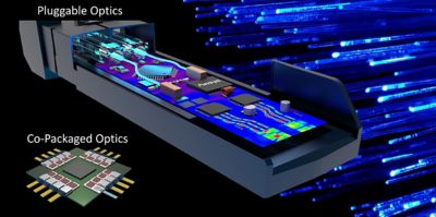
Comparison of pluggable optics versus co-packaged optics
Reaping the Benefits of Co-packaged Optics
Early CPO solutions from Broadcom and Cisco show 30-50% in power consumption savings, with interconnection power of about <1 pJ/bit. Ayar Labs has demonstrated 16 Tbps of bidirectional throughput at <5 pJ/bit. Generally, CPOs offer power saving in several different ways:
- No lossy copper traces: Unlike pluggable optics, CPO design eliminates the need for signals to traverse from the application-specific integrated circuit (ASIC) chip over energy-sapping copper links across the board up to the front panel. Instead, CPO design brings the fiber directly to the switch enabling short, low-loss communication between the chip and the optical engine.
- Fewer digital signal processors (DSPs): In current architectures for speeds higher than 25G/lane, DSP-based retimers have become necessary components in pluggable optics to actively analyze and compensate for signal degradation, distortions, and timing issues. The DSP contributes to driving up the overall system power by as much as 25-30%. However, given that CPOs eliminate the off-chip lossy copper traces between the ASIC and the optics, designers can safely eliminate one DSP level to save power and reduce costs.
- Integrated lasers: There are two schools of thought regarding laser source placement. The prevalent approach involves an external laser, necessitating the transmission of light through a fiber and coupling it into the CPO and typically incurring an optical power loss of 30-50%. The alternative approach integrates the laser directly onto the chip, offering a notably higher optical coupling compared to the latter approach, provided that thermal management and laser reliability are viable.
- High bandwidth and low latency: CPOs can enable higher bandwidth and lower latency, mainly because of fewer DSPs and the removal of long copper traces. Additional blocks like DSPs as well as the parasitics in copper traces all introduce delays that signals won’t see in a CPO solution.
Applying Co-packaged Optics
CPO for networking: The primary application of CPOs is in front-end networks used for connecting servers in data centers. Due to the high bandwidth, low latency, and power efficiency benefits described above, CPOs are a promising approach to implementing the next generation of optical ethernet technology for networking applications.
OIO (HPC for AI/ML): To handle AI/ML workloads, the optics industry is investigating a new fabric called the AI back-end network that is enabled by OIOs.
In computing, the challenges of inflexible resource allocation in traditional, siloed HPC architectures converge with the longstanding limitations of data transfer rates, creating notable bottlenecks in bandwidth capacity and inefficiencies in handling workload diversity. As processing speeds of central processing units (CPUs) and graphics processing units (GPUs) surge ahead, the existing I/O infrastructure is struggling to keep pace, leading to inefficiencies where processing units frequently wait for data.
This predicament becomes even more critical with the escalating demands of AI/ML workloads, which necessitate a network fabric characterized by high speed, low latency, lossless data transfer, and scalability. Herein lies the significance of OIOs, which are poised to revolutionize the status quo.
The evolving disaggregated architecture in HPC endeavors to overcome the siloed constraints by separating memory, compute, and storage into clusters interconnected by cutting-edge OIO. This strategic shift enables dynamic resource allocation, addressing the inefficiencies of traditional architectures when dealing with diverse data center workloads.

The primary application of CPOs is in front-end networks used for connecting servers in data centers.
Understanding the Challenges of Co-packaged Optics
- Vendor lock-in: A situation in which the switch and optics are supplied by a single vendor implies a potential lack of flexibility and freedom for the hyperscaler. Once they invest heavily in a specific vendor's ecosystem, they may face difficulties transitioning to another vendor's products. This can limit their ability to easily switch or upgrade components, potentially leading to dependencies and constraints.
- Reliability and field serviceability: Pluggables are highly modular and can swiftly be replaced in the event of failure or be swapped in and out from any vendor. In CPOs, replacing optics involves pulling out the entire switch, requiring a level of expertise to perform a complex service task. To address this challenge, some CPO designs disaggregate high-risk active components like lasers onto a remote pluggable module that is more easily field-replaceable. Others are looking at pluggable optical connectors.
- Thermal management: The placement of the photonic integrated circuit (PIC) inside the electrical package increases the possibility of thermal crosstalk. While the thermal power from heaters and laser sources in the photonic die will affect the temperature map of the package, the heat generated in the electrical dies and the cooling mechanism of the overall system will affect the thermal behavior of the PIC. A complete thermal analysis from die to system level is therefore needed.
- Signal integrity and power integrity: Transient simulation of the entire system is needed to ensure signal and power integrity. This will require self-consistent electrical and photonic circuit simulations while accounting for the additional parasitic effects coming from the different types of electrical interconnects introduced at the packaging stage.
- Scalability and beachfront: A key metric for CPO and OIOs is the beachfront, or the bandwidth density along the edge of the chip, as fibers are typically edge coupled. There are minimum fiber spacing requirements that limit the number of fibers for a given substrate size. Given the large discrepancy between waveguide and fiber dimensions, fan-out becomes an inherent challenge for edge-coupled solutions. Now imagine having to accommodate several thousands of fibers without blowing up the substrate size. Using V-grooves enables vertically orienting the fiber for an edge-coupled solution without fan-out. Grating-based coupling with microlenses is also being investigated along with other innovative solutions.
- Fiber attachment: Efficient coupling of the optical signal from the fiber array to the package is a challenging task. There are several considerations such as fiber alignment (achieved via passive or active alignment methods) and tilt, structural and thermal management, manufacturability, and serviceability. Designers will need to carefully model and optimize their optical coupling designs.
- Manufacturability and testability: Low costs and high yield are what make a design commercially viable. Especially in a multivendor supply chain, consistent quality and effective testing procedures are essential hurdles that will continue to develop with demand and investment.

The placement of the photonic integrated circuit (PIC) inside the electrical package increases the possibility of thermal crosstalk.
Examining Relevant Market Trends
The emergence of chiplets: Chiplets are essentially small individual dies that can be co-packaged to operate as a single chip, shifting the industry from systems on chip to a system of chips in one package. Chiplets can potentially play a role in or even accelerate CPO adoption. The chiplet approach enables the mixing of different technologies and functionalities in one package. For example, the OIO chiplet could be based on an older CMOS node, whereas the ASIC is on a more advanced node enabling lower costs and better die yields.
Integration density via 3D-IC: The semiconductor industry is experiencing integration density advancements through 3D-IC technology. Though many CPO approaches today include placing an optical and electrical chip next to each other on a low-loss substrate, advancements in 3D-IC can enable a multi-die chiplet CPO in which the OIOs and ASIC are integrated in 3D using very low power and very high-bandwidth inter-chip communications. This integration density results in larger and more complex designs, which requires an increasing need for multiphysics and electromagnetic (EM) simulations to analyze new emerging physical effects.
Linear drive pluggable optics (LPOs): The incumbent pluggable technology isn’t going to give up without a fight. Similar to CPOs, LPOs offer power savings by removing the DSP from pluggable optics. The close placement of optics and electronics in CPOs have driven a few orders of magnitude of miniaturization over traditional pluggable modules. However, this miniaturization can also be adopted by pluggables themselves to improve their bulky form factor.
Meeting market expectations and gaining end-user confidence in the viability of CPO requires the demonstration of robust multi-vendor business models and significant cost and power savings. To leverage the industry trends and technologies for accelerated adoption of CPO and OIOs, the optics community needs to put into place some essential missing pieces such as IP blocks and standards for the optics interfaces. Collaborations across all players in the supply chain are necessary, from design and simulation software providers, device and chip designers, and system architectures to packaging houses, test equipment providers, and foundries. Bringing up an ecosystem is no small endeavor that will surely take time. Nevertheless, with the arrival of colossal applications like AI/ML, the race is on.
For more information on modeling co-packaged optics visit our Optics Product Collection page and our application gallery, which features a large collection of examples such as modeling of an integrated microlens and grating coupler for photonic integrated circuits.