Synopsys and Ansys power the future of innovation—connecting silicon to systems.

Our personal devices are evolving to better fit consumer preferences. Smartphone cameras are slimming down. Augmented reality (AR) headsets are becoming increasingly lighter and more comfortable. And automotive technologies are shrinking to fit within the complex systems they support.
All this is made possible by the shrinking of optical systems and their individual elements, including lenses, beam shapers, and sensors, is the trend driving this growth. The optics and photonics market size was valued at USD 1,049.5 billion in 2025, and it is expected to reach USD 1,994 billon by 2035, with a CAGR of 6.7% from 2025 to 2035.
Now, emerging technologies like photonic integrated circuits and metasurfaces, including metalenses, are replacing bulky traditional optics. They’re specifically intended to overcome size limitations, expand device functionality, and improve energy efficiency.

Simulation-driven design of photonic integrated circuits enables engineers to model light behavior and optimize performance at the nanoscale.
To design on this scale requires higher precision, as optical engineers face new constraints, including tighter tolerances and complex light-matter interactions. It also involves rethinking both manufacturing processes and materials to ensure the successful integration of these imperceptibly small systems into existing devices.
To do this, what optical engineers really need are sophisticated simulation tools to design, evaluate, and manufacture these technologies on the nanoscale.
Simulation excels at replicating real-world scenarios. It enables optical engineers to consider system performance subject to different environmental factors, assembly tolerances, or material properties. Additionally, iterative design adjustments can then be made without any of the typical delays expected during the fabrication of multiple prototypes.
“From refining nanoscale components to assessing large-scale system performance, simulation offers an unparalleled platform for exploring new optical possibilities and ensuring reliability in compact, high-performance designs,” says Yifan Yuan, staff engineer, applications engineering at Ansys, part of Synopsys.
Assessing Nanoscale Designs With Macroscale Functionality, Virtually
A number of intricate design challenges come with miniaturization. Among them are the need for precision during system alignment, the management of tighter tolerances, and the ability to maintain performance in a much smaller form factor. In an attempt to solve them, traditional engineering approaches bump up against the limitations of physical prototyping, as well as the complexities involved in scaling down optical components.
However, this is where simulation really shines.
Take, for example, the challenge of modeling how light interacts with subwavelength features. At the component level, Ansys Lumerical FDTD software can accurately capture these interactions for nanostructures like meta-atoms in metalenses. And system-level tools like Ansys Zemax OpticStudio software can assess how miniaturized optical elements integrate into larger assemblies. Understanding these relationships leads to accurate predictions of potential misalignments or performance degradation before manufacturing begins.
Then there’s the challenge of balancing trade-offs among high numerical aperture and field of view or chromatic aberrations and complexity. Using simulation, optical engineers can explore these trade-offs to arrive at data-backed insights that ultimately lead to better design decisions.
“By incorporating advanced simulation techniques, engineers can tackle miniaturization challenges, ensuring functional integrity and efficient design workflows for compact, integrated optical solutions,” says Yuan.
Slimming Down Metalenses on the Nanoscale
One of the hottest trends in optics is metalenses, which rely on precisely arranged subwavelength nanostructures to support size reduction and high performance. Equally flat and lightweight, these components are ideal in the pursuit of compactness without compromising on functionality.
Basically, metalenses shed their bulky curves for thinner surfaces that can better manipulate light through phase control at the nanoscale. The result is thinner, more versatile optical designs.

Advanced nanofabrication enables the production of metasurfaces and metalenses optimized through simulation-driven design.
But like other subwavelength structures, metalenses demand meticulous attention to geometric parameters during development, including height, radius, and spacing, as each influences the phase and transmission of light. Subsequently, advanced simulation techniques are required for their accurate characterization and optimization.
Tools like FDTD software enable rigorous simulation methods, such as finite difference time-domain (FDTD) and rigorous coupled-wave analysis (RCWA), to model these interactions. And, using OpticStudio software, it’s possible to bridge the gap between nanoscale design and macroscale performance to successfully evaluate metalens concepts within a complete system.
“By combining Lumerical software for nanoscale meta-atom analysis and OpticStudio for system-level refinement, engineers can efficiently design and integrate metalenses into optical systems, connecting simulation with real-world applications,” says Yuan.
Optimizing Manufacturing With Process Design Kits (PDKs)
Ansys, part of Synopsys, and Moxtek partnered to develop a PDK that integrates FDTD software and OpticStudio software with Moxtek’s nano-fabrication capabilities. PDKs serve as part of a standardized tool set for the efficient modeling, simulation, and fabrication of advanced metasurfaces in the Moxtek nano-foundry.
Essentially, PDKs are used to forge a connection between the theoretical and the practical — that is, between metalens designs and fabrication by the integration of simulation and real-world manufacturing parameters.
“The Moxtek/Ansys Process Design Kit streamlines the design-to-fabrication process by integrating nano-fabrication rules and validated libraries, significantly reducing iterations and enhancing efficiency during optical miniaturization,” says Yuan.
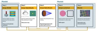
A simulation-driven metalens workflow showing how rigorous coupled-wave analysis (RCWA), Ansys Zemax OpticStudio optical system design and analysis software, and Ansys Lumerical tools connect nanoscale meta-atom design to system performance and fabrication
By simulating the effects of manufacturing processes on metalens production contextualized within the PDK, optical engineers can learn a lot. The PDK offers insights into common challenges that impact performance, such as corner rounding (rounding edges for improved function/aesthetics) or pitch shifts (manipulations of the pitch size). The overarching idea here, of course, is to fine-tune metalens design optimization to align with production and functional objectives.
Furthermore, the seamless integration of PDKs with simulation tools like FDTD software and OpticStudio software enables engineers to get ahead of any manufacturing considerations early in the design phase. As a result, discrepancies that often happen between simulated performance and fabrication devices can be minimized early on, reducing scrap and costs during production.
Trending Smaller With Simulation
Miniaturized optics are part of an upward trajectory for smaller, lighter optics, which are delivering superior performance compared with their former, bulky counterparts. As the demand for smaller high-performance optics continues to grow, so will the need for simulation.
To learn more about our solutions, make sure to download the Ansys Optics Miniaturization Solutions e-book.
Just for you. We have some additional resources you may enjoy.


The Advantage Blog
The Ansys Advantage blog, featuring contributions from Ansys and other technology experts, keeps you updated on how Ansys simulation is powering innovation that drives human advancement.