-
-
Software gratuito per studenti
Ansys potenzia la nuova generazione di ingegneri
Gli studenti hanno accesso gratuito a software di simulazione di livello mondiale.
-
Connettiti subito con Ansys!
Progetta il tuo futuro
Connettiti a Ansys per scoprire come la simulazione può potenziare la tua prossima innovazione.
Paesi e regioni
Customer Center
Supporto
Partner Community
Contatta l'ufficio vendite
Per Stati Uniti e Canada
Accedi
Prove Gratuite
Prodotti & Servizi
Scopri
Chi Siamo
Back
Prodotti & Servizi
Back
Scopri
Ansys potenzia la nuova generazione di ingegneri
Gli studenti hanno accesso gratuito a software di simulazione di livello mondiale.
Back
Chi Siamo
Progetta il tuo futuro
Connettiti a Ansys per scoprire come la simulazione può potenziare la tua prossima innovazione.
Customer Center
Supporto
Partner Community
Contatta l'ufficio vendite
Per Stati Uniti e Canada
Accedi
Prove Gratuite
ANSYS BLOG
May 25, 2023
Transformation in the Photonics Industry
The photonics industry is experiencing serious growth across its core application areas, and there’s a lot of pressure to produce from both a quality and quantity perspective. Let's think through the many technical factors driving transformation in the photonics space.
Component Miniaturization
Whether due to weight restrictions or size constraints, there’s a need for smaller system designs throughout the optics space. While cost is always a consideration, engineers are carefully assessing the trade-offs between more expensive, complex technologies and the potentially immense benefits to shrinking size.
A great example of this is the emergence of so-called "flat lenses." By customizing the behavior of light as it passes through specially designed microstructures located either on the surface or within the lens, complex geometries and curvatures are no longer central to achieving high-quality performance. While flat lenses are not (as their name might suggest) perfectly flat, they offer more opportunities to tailor optics for high performance while reducing size and weight. Recent designs demonstrate that flat lenses can work well at a single wavelength, but they’re still not quite as effective as traditional lenses when working across multiple wavelengths. But, as always, the industry continues to innovate!

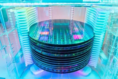
Efforts to miniaturize are happening across the optics space, and the more engineers understand how to work with and manufacture small-scale components, the more mainstream these components will become in optical product design. Considering companies are already using technology like photolithography to manufacture semiconductor chips, we will start to see small-scale component manufacturing translate into manufacturing of small optical components. Many companies are already manufacturing optics on a chip.
Desire to Scale
Optics plays a central role in many emerging technologies. Take lidar systems in automobiles, for example. To get to the point where there are millions of these systems on the road, vehicles can no longer have bulky, expensive spinning tops with lots of failure-prone mechanical parts. Lidar must be integrated into the vehicle, and the use of integrated photonics will make that easier to accomplish at scale. Companies like Lumotive and Scantinel are already doing it.

Integrated photonics or the aforementioned flat lenses can help cell phones and other consumer electronic devices overcome limitations, too. Much of what sets the thickness and size of a mobile display is related to optics and optomechanics, but lenses and lens mounts add bulk. Looking ahead, designs could feature injection-molded plastic lenses with custom mechanical mounting edges that can be snapped into place during assembly. That design feature could eliminate the need for those bulky optomechanical mounts and holders. By swapping some traditional lenses for flat lenses, could these designs achieve the high image quality consumers want in a smaller form factor?
Use Hardware and Software for Performance Optimizations
Engineers are turning to advanced software to fine tune the performance of their hardware systems. For example, the Google Pixel 6 camera combines hardware, software, and machine learning to offer high-quality capture and editing tools like Magic Eraser in Google Photos.
The tension between good, better, and best presents software and hardware design trade-offs. For example, opting for a good hardware system with off-the-shelf components and focusing on a best-level software system could save hardware costs and still achieve the desired result. However, higher computational costs translate to higher power requirements. Engineers need to be able to explore the outcomes of their design decisions.
In industries with more regulation and a higher cost of error, like automotive and healthcare, it’s harder to make those trade-offs. In these applications, technologies like AI-enabled computer vision aren’t advanced enough for trusted results yet, so there’s a greater focus on making traditional, documented design processes faster, easier, and more cost effective through automated workflow tools.
Changing Workflows in Service of Transformation
To keep up with industry-level transformation, companies need to change the way they work. A typical workflow includes design, analysis, multiple tolerance studies, mechanical design, communication with manufacturing, manufacturing preparation, and production. Engineers using more than one tool for design and simulation end up spending much — if not most — of their time figuring out how to move data accurately between tools. How can we bring uniformity to data models and prevent these kinds of inefficiencies? One answer is better workflows, and another is defining and supporting standards where it makes sense to do so.
But how do engineers make sure they’re designing a product that’s going to perform as well in the real world as it does in virtual design? That’s still the central question. For simulation providers, that question translates to: How can we make sure engineers feel confident in their designs? Confidence inspires meaningful innovation and creativity, and we need that.
For the design of modern products, simulation tools must enable engineers to conduct comprehensive multiphysics modeling in an integrated and streamlined manner. Engineers need tools that work together in an open development ecosystem to support customization and automation. Ansys understands these challenging requirements and addresses them with a diverse product portfolio that can be connected through built-in scripting and analysis automation tools to support engineers from design through manufacture. Simulating performance through digital prototyping helps engineers uncover problem areas before the time and expense of manufacturing.

Defining and Supporting Standards
In some application areas, the optics industry is ripe for standards that can bring it to scale, but with rapid innovation, it’s understandable that companies worry about losing their competitive edge. Creating an optics product development ecosystem will require industry collaboration — there’s no getting around it. To make that happen, Ansys, as a simulation provider, is working to make it easier for companies to adopt consistent best practices for design.
As growth in the photonics industry continues to grow, we challenge engineering simulation technologists to take a bird’s-eye view. How can simulation providers encourage collaboration and innovation while fostering and supporting proprietary technologies?
See how Ansys Optics and Ansys Photonics can help you.