-
-
Software gratuito per studenti
Ansys potenzia la nuova generazione di ingegneri
Gli studenti hanno accesso gratuito a software di simulazione di livello mondiale.
-
Connettiti subito con Ansys!
Progetta il tuo futuro
Connettiti a Ansys per scoprire come la simulazione può potenziare la tua prossima innovazione.
Customer Center
Supporto
Partner Community
Contatta l'ufficio vendite
Per Stati Uniti e Canada
Accedi
Prove Gratuite
Prodotti & Servizi
Scopri
Chi Siamo
Back
Prodotti & Servizi
Back
Scopri
Ansys potenzia la nuova generazione di ingegneri
Gli studenti hanno accesso gratuito a software di simulazione di livello mondiale.
Back
Chi Siamo
Progetta il tuo futuro
Connettiti a Ansys per scoprire come la simulazione può potenziare la tua prossima innovazione.
Customer Center
Supporto
Partner Community
Contatta l'ufficio vendite
Per Stati Uniti e Canada
Accedi
Prove Gratuite
ANSYS BLOG
February 28, 2022
Simulate to Mitigate Electrostatic Discharge on Spacecraft
In space, there is no atmosphere to protect spacecraft from radiation. Charge buildup from the radiation can’t dissipate because the spacecraft are not grounded to Earth. So, spacecraft design must properly mitigate charge accumulation and dissipation on the spacecraft’s surface and inside components.
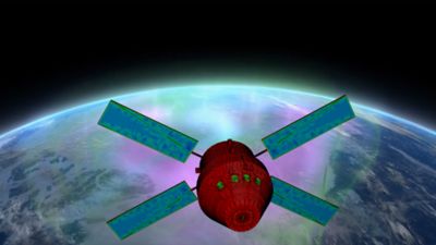
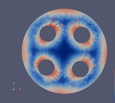
Figure 1: Charging simulation in EMA3D Charge of a human space capsule in a geostationary orbit (GEO) environment.
When charge accumulates, it induces electric fields. The magnitude of the electric fields may exceed the breakdown of air, plasmas, or dielectrics and lead to electrostatic discharges (ESDs). The damage from discharges can cause total mission failures.
ADEOS-II — a $567 million mission — failed in October 2003 due to an arc in the solar arrays. And this failure is not an isolated event. Roughly 50% of space environment spacecraft anomalies are caused by spacecraft charging effects.1

Figure 2: Conceptual diagram of physical processes involved in spacecraft charging.
Design standards are put in place by NASA and ESA to preemptively mitigate these spacecraft charging concerns. For the private sector, meeting these standards can be expensive and time consuming. Pushing the limits of design requires accurate charge simulation tools, such as Ansys EMA3D Charge.
Surface Charging
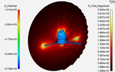
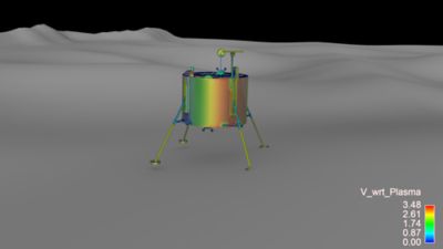
Figure 4: Above, the results of the surface charging simulation of a human space capsule. The electric field is monitored in the time domain, in 3D, around the spacecraft. Below, the effect of solar illumination on a high-resolution mesh of a lunar lander.
Surface charging comes from a material response to external radiation such as ambient charged particles, photo-illumination, and tribo-electrification. The material response to the charging effects depends on the material’s properties. The resulting photoelectrons, secondary electrons, back-scattered electrons, and proton-induced electrons interact with the electric fields to form a plasma sheath. Surface potentials with respect to the plasma may exceed 10 kV in some spacecraft orbital environments. By solving for that balance of charge, EMA3D Charge provides the means to analyze surface charging of spacecraft.
On the way to the Moon, spacecraft will encounter surface charging effects of varying scales depending on their transfer orbits. Geostationary orbit (GEO), low-Earth orbit (LEO), Polar, Auroral, and Lunar orbits will all have different plasma environments defined in the design-specification standards. Geometry, shadows, and the material properties, in addition to the plasma properties or the tribo-electrification amplitude, play a role in the charge accumulated at the surface of the spacecraft. With a high-fidelity mesh, you do not have to omit significant details from your models. The lunar lander and human space capsule’s circular windows, sensors, antennas, and thrusters can all be meshed with enough fidelity to precisely isolate areas of concern for ESDs.
Internal Charging
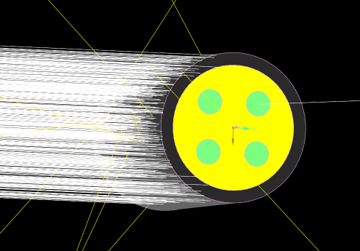
Figure 5: Above, high energy electrons are shined on a shielded pin connector. Scattered particles and secondary photons are created when electrons interact with the built material. Below, the electric field in the dielectric surrounding the pins reached levels that are near the dielectric strength of a typical insulator.
Internal dielectric charging results from the interaction of charged particles from the sun (and high energy photons) and the bulk material of the spacecraft. These particles may be accelerated by solar flares or by the Earth’s magnetic field such as in the Van Allen belts or near the poles. The charge deposited by these particles induces fields that can lead to dielectric breakdown. By modeling the charge deposition rate and magnitude, engineers can refine their radiation hardening designs, estimate the risk of ESD, and simulate currents induced on electronics.
In plasma environments where the energy of charged particles is high enough to result in deep dielectric charging, EMC engineers must be concerned with the risk of charge accumulation inside sensitive components such as solar cells, sensors, and exposed cables or connectors. To assess the risk of ESD in a dielectric, EMA3D Charge couples a 3D particle transport tool with a full-wave finite element method (FEM) solution of electromagnetism solved in the time domain. With this method, engineers can monitor potential, fields, charge, and currents induced by the interaction of particles with bulk materials. The particles can be incident upon a variety of geometric configurations, their energy spectrum can be time dependent, and multiple types of particles can be simulated at once. To tackle the applications presented as examples, EMA3D Charge has refined mesh algorithms (such as extrusions) to ensure the proper fidelity when simulating numerous thin layers or long cables with complex shield designs. A high-resolution simulation of electric fields in 1-mil thick layers is necessary to isolate the critical region at risk of ESDs.
Solid Dielectric Breakdown
Figure 6: A metal rivet connected to a ground plane is placed in a glass dielectric. High energy electrons are deposited on the top of the glass and image charges build up on the tip of the rivet. The resulting fields are high enough to breakdown glass.
If there is too much charge in the system, then the resulting electric fields will exceed the breakdown threshold of the medium. Discharges occur from the spacecraft to the plasma, from one conductor to another across plasma, air, or directly inside a dielectric/insulator. At worse, these discharges can lead to secondary arcing if the spacecraft isn’t well grounded, and a situation similar to that of ADEOS-II can occur. Additionally, ESDs radiate electromagnetic radiation, which can be damaging to communication systems. For example, too much charge accumulated in a cable connected to sensitive electronics may induce currents that will damage the instruments. In some cases, due to design constraints, you will have to accept a minimal amount of primary arcing in your spacecraft. In other instances, a design tailored for a specific radiation environment such as LEO may need to be reused in a harsher radiation environment such as GEO.
To simulate dielectric breakdown (a process that occurs at nanosecond time scales), EMA3D Charge leverages a full-wave electromagnetic solver and a stochastic tree model that calculates the probability of breakdown as a function of electric field, dielectric strength of the material, and coupling strength to adjacent nodes. That probability distribution is evaluated at each time step and at each node of the FEM mesh used for the problem.
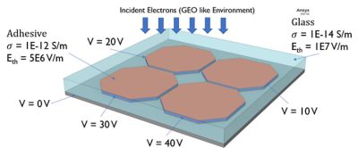
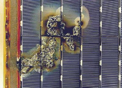
Figure 7: Above, the model setup for the breakdown of a solar cell coupon with the bias voltage applied to each cell and with the properties of the materials. Electrons from a geosynchronous (GEO) environment were shined from the top with a planar geometry. Below, an image of real damage resulting from dielectric breakdown of solar cells.
As a demonstration of this simulation capability, the solar cell coupon presented in Figure 7 is ideal to exemplify concerns associated with the charging of solar panels in space. The four solar cells are placed on a conductive backing and are each assigned a different voltage bias. A thin adhesive layer is placed at the bottom and top of each cell. A glass substrate is placed on top of the cells for electrical and mechanical protection. In GEO, high-energy electrons will deposit at the top of the substrate and image charges will build on the solar cells. In this design, the resulting electric field that is enhanced by the geometry of the cells turns out to be high enough for dielectric breakdown of glass.
With EMA3D Charge, the full-wave electromagnetic solver and the 3D particle transport co-simulate on the same FEM mesh. After sufficient time in this high-radiation environment, the electric field exceeds the breakdown strength of glass, and the stochastic tree model is activated to simulate the breakdown process.
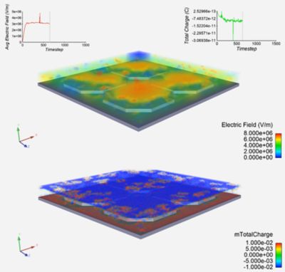
Figure 8: On the top, line plots of the average electric field and the total charge through time. In the middle, a 3D color map of the electric field after 700 timesteps. On the bottom, a 3D map of the charge density in the glass.
The snapshots of the results displayed in Figure 8 showcase the arcing damage on the model. Discharges first occur on the edges of the cells when the average electric field reaches 3x10⁶ V/m. The highly conductive arc channels dissipate any further deposited charge. Over time, the post breakdown conductivity dominates over the glass conductivity, leading to a lower electric field equilibrium. The charge density map shows the negative charge layer due to the incident electrons. Positive image charges form on the edges of the cell and bottom substrate while negative charges form on the top of the adhesive. This led to the enhancement of the electric field on the cell edges resulting in multiple simultaneous breakdowns. As the breakdowns occur, they dissipate the space charge deposited by the high-energy electron plasma, which slowly lowers the total charge in the model. By looking at the change in energy and charge before and after a discharge, we can calculate their averages. The average charge was 117 nC, and the average energy was 19 mJ.
To tackle the applications described above, Ansys EMA3D Charge leverages multiple physics solvers capable of co-simulations: a surface charge balance solver, a full-wave FEM solution of electromagnetism, and a 3D particle transport tool. By offering a means to simulate charge accumulations and dissipations accurately and in detail for a broad variety of instruments, materials and orbital targets, Ansys EMA3D Charge helps design teams develop more robust space platforms and maximizes the probability of long-term success for these expensive programs.
Learn more about Ansys EMA3D Charge platform-level EMC cable modeling.
1. "The Impact of the Space Environment on Space Systems," H. C. Koons, J. E. Mazur, R. S. Selesnick, J. B. Blake, J. F. Fennell, J. L. Roeder, and P. C. Anderson; Space and Environment Technology Center Technology Operations; July 20, 1999