ANSYS BLOG
February 25, 2021
A Better Way to Design CMOS Image Sensor Cameras
Ansys now offers a better way to design CMOS image sensor cameras enabled by the interoperability between its Lumerical and Speos tools. Engineers can now optimize the efficiency of the CMOS sensor in conjunction with the additional macroscopic lens and electronics subsystems of the camera. The workflow enables engineers to optimize CMOS image sensors while considering realistic illumination conditions.
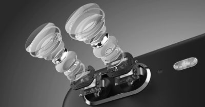
Commonly used in today’s digital cameras and mobile phones, CMOS image sensors leverage existing CMOS manufacturing processes and have become the low-cost approach for image sensing.
Ansys Speos is used to predict the illumination and optical performance of systems. Speos enables engineers to study the interaction of light with mechanical geometries at a macro scale, saving on prototyping time and costs.
Ansys Lumerical provides nano-photonic simulation tools that enable users to model the interaction of light with geometries at wavelength scale, including optical, electrical and thermal effects.
Speos and Lumerical can share simulation information for a variety of applications, such as heads-up displays (HUDs), systems with plasmonic surfaces, diffraction gratings, emissive structures, surface and volume scattering and diffractive optical elements. The new workflow for CMOS sensor cameras is one more addition to this growing list of applications where the combination of Speos and Lumerical tools offer simulation solutions for complete optical systems.
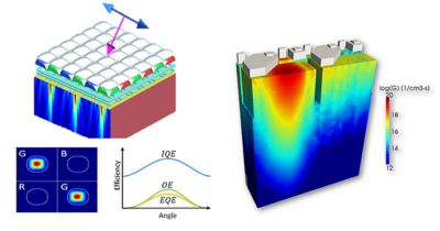
A CMOS image sensor modeled in Ansys Lumerical FDTD (left) and Lumerical CHARGE (right).
CMOS Image Sensor Cameras
Ansys Lumerical FDTD can be used to model optical properties of nanophotonic devices such as CMOS image sensors. Key properties available to engineers include the optical efficiency of photon absorption and electron-hole pair generation rate in the substrate. Coupled with Ansys Lumerical CHARGE, designers can explore other import properties such as quantum efficiency and crosstalk which both require the simulation of electrical behavior. Ansys Lumerical’s FDTD and CHARGE can be used to tackle design challenges such as backside illumination, the impact of optical and electrical crosstalk, the optimization of microlens shift or geometry for oblique angles of incidence, and the effect of color filters when incorporated into complicated sensor geometries.
When coupled with Ansys Speos, engineers can take CMOS image sensor camera design to the next level by simulating the entire camera system. This enables users to explore the complex interplay among the microscopic effects of CMOS image sensors, the macroscopic lens and electronic subsystems. With its ability to predict illumination performance, Speos enables engineers to construct an accurate view of the final image as recorded by the camera.
Whether designing the camera for a next-generation mobile phone or the imaging system for scientific or defense applications, a Speos/Lumerical workflow can help you create better CMOS image sensor cameras faster and cheaper.
Get a free trial of Ansys Speos today!