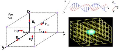
Quick Specs
A range of benefits allow for flexible and customizable models and simulations. Ansys Lumerical FDTD models nanophotonic devices, processes and materials so you can focus on creation.
Ansys Lumerical FDTD is the gold-standard for modeling nanophotonic devices, processes, and materials. The integrated design environment provides scripting capability, advanced post-processing, and optimization routines.
Lumerical FDTD: Reliable, Powerful and Scalable Solver Performance
This finely tuned implementation of the FDTD method delivers best-in-class solver performance over a broad spectrum of applications. The integrated design environment provides scripting capability, advanced post-processing and optimization routines, allowing you to focus on your design and leave the rest to us.
A range of benefits allow for flexible and customizable models and simulations. Ansys Lumerical FDTD models nanophotonic devices, processes and materials so you can focus on creation.
JULY 2023
The 2023 R2 release introduces new FDTD simulation performance acceleration using a single GPU, new features for advanced CMOS image sensor design, and enhanced flexibility for defining geometries using the layer builder feature.
GPU enables faster FDTD simulations with parallelization on the graphic card. A single GPU Nvidia RTX4000 can offer a 6x speedup. This first version of GPU-supported FDTD runs on a constrained set of resources, monitors, and materials behaviors compatible with a single GPU.
This new feature in Lumerical Multiphysics Suite supports operations between any mask layers. Enables cases where a combination of multiple mask layers determines the geometry.
FDTD includes the marginal rays from OpticStudio in the pixel simulation for an accurate calculation of the quantum efficiency. The EQE vs. subpixel position and wavelength is combined with Speos light exposure and post-processed by the new Speos sensor system to see all intermediate and final electronic images.
CAPABILITIES
Lumerical FDTD is the gold-standard for modeling nanophotonic devices, processes and materials. This finely tuned implementation of the FDTD method delivers reliable, powerful and scalable solver performance over a broad spectrum of applications. The integrated design environment provides scripting capability, advanced post-processing and optimization routines, allowing you to focus on your design and leave the rest to us.
Automatically discover optimal designs and geometries for a targeted design goal. Discover non-intuitive geometries that optimize performance, minimize area, and improve manufacturability.
Powerful post-processing capability, including far-field projection, band structure analysis, bidirectional scattering distribution function (BSDF) generation, Q-factor analysis, and charge generation rate.
Simulate devices fabricated with nonlinear materials or materials with spatially varying anisotropy. Choose from a wide range of nonlinear, negative index, and gain models. Define new material models with flexible material plug-ins.
Uses multi-coefficient models for accurate material modeling over large wavelengths ranges. Automatically generate models from sample data or define the functions yourself.
FDTD’s CAD environment and parameterizable simulation objects allow for rapid model iterations for 2D and 3D models.
It's vital to Ansys that all users, including those with disabilities, can access our products. As such, we endeavor to follow accessibility requirements based on the US Access Board (Section 508), Web Content Accessibility Guidelines (WCAG), and the current format of the Voluntary Product Accessibility Template (VPAT).