Skip to Main Content

Ansys PathFinder-SC
Electrostatic Discharge (ESD) Simulation Software

Ansys PathFinder-SC is a high-capacity solution to help you plan, verify and sign-off IP and full-chip SoC designs for integrity and robustness against electrostatic discharge (ESD).

ESD SIGNOFF

Full-Chip Layout Level ESD Signoff Solution for SOC IP

Ansys PathFinder-SC identifies and isolates the root causes of design issues that can cause chip failure from charged-device model (CDM), human body model (HBM), or other ESD events. It’s high-capacity, cloud-native architecture can enlist thousands of compute cores for fast full-chip turnaround. PathFinder-SC is certified by major foundries for resistance and current density checks for ESD signoff.

  • Integrated with Totem-SC Power Integrity
    Integrated with Ansys RedHawk-SC™ and Ansys Totem™
  • Outputs Chip ESD Compact Model (CECM)
    Outputs Chip ESD Compact Model (CECM)
Full-Chip ESD Signoff Solution for Layout and Circuit Levels

Quick Specs

PathFinder-SC’s integrated data modeling, extraction and transient simulation engine is an end-to end solution for ESD verification. The single-pass use model reads industry-standard design formats, sets up ESD rules, extracts the RCs for the power network, and performs ESD simulations to analyze root causes and provide fix and optimization feedback, all within a single tool.

  • CDM & HBM Coverage
  • P2P Resistance Checks
  • Current Density and IR Checks
  • GDS and Digital Flow Support
  • Cloud-native Architecture
  • Analyze Multiple Domains in a Single Run
  • Handles Snap-back ESD
  • More Than 100 Million Instance Capacity
  • Layout GUI for Debug
  • Compact ESD Model for IP
2020-11-ansys-stock-20190114-0037-horizontal.png

Electrostatic discharge and current density are key factors that determine a chip’s real-world robustness and its long-term reliability. These are critical for product safety and durability.

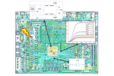
Lowering device breakdown voltages and interconnect dimensions poses increased ESD risk in sub 16nm processes. PathFinder-SC offers comprehensive analysis of on-chip ESD events, which is a requirement for all chip designs.

PathFinder-SC’s full-chip capacity and streamlined, single-pass use model can simultaneously handle hundreds of domains in one analysis. This is significantly faster than traditional approaches, speeding the time to results and reducing the potential for errors due to partitioning.

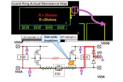
Any detected issues can be quickly debugged with PathFinder-SC’s layout-based analysis and Root Cause Detection technology, once again saving time and speeding time to market.

PathFinder-SC includes all capabilities in a single product – from performing RC extraction and ESD simulations, to analyzing root cause and providing optimization feedback. It includes a built-in RC extractor and requires no extra licenses or external tools.

PathFinder-SC is silicon-correlated by several customers and validated by multiple foundries which ensures accuracy and reduces silicon risk.

Comprehensive electrostatic discharge (ESD) solution for analysis, debug and optimization of IC layout and circuits

Ansys PathFinder-SC helps you plan, verify and sign-off IP and full-chip SoC designs for integrity and robustness against ESD. It identifies design issues that can cause chip or IP failure from charged-device model (CDM), human body model (HBM) or other ESD events. PathFinder-SC is certified by major foundries, assuring that interconnect parasitics, HBM/CDM ESD simulation, and resistance and current-density checks are accurate for ESD signoff. It’s layout-based GUI facilitates fast root cause detection and easy debugging.

PathFinder-SC is architected with a cloud-native infrastructure that enables elastic computing and the ability to handle full-chip analyses of over 100 million transistors.

Key Features

Full-chip and comprehensive single-pass ESD analysis and debug for hundreds of power modes, simultaneously. 

  • HBM/CDM ESD Events
  • Silicon-Correlated Accuracy
  • Root Cause Detection
  • Single Pass Simulation
  • Capacity and Performance
  • Library to SoC-Level
  • Cloud-Native Elastic Compute

Ansys PathFinder-SC mimics human body model (HBM) and charged-device model (CDM) ESD events by propagating the zap current through power/ground networks to identify layout bottlenecks. It models the injection of current into any pad and interconnect pathway to identify pin-clamp-pin paths that cannot handle high ESD currents.

Ansys PathFinder-SC’s transient simulations using SPICE models and TLP curves at picosecond resolution offer silicon-correlated accuracy, which helps to minimize your design risk. Clamps with snap-back often have convergence issues in SPICE; but PathFinder-SC’s simulation engine is customized to handle snap-back and accurately model ESD device triggering. PathFinder’s results have been correlated with silicon by multiple foundries and customers.

Ansys PathFinder-SC identifies layout issues and connectivity imbalances that may lead to ESD failure. Examples include bumps not connected to ESD clamps, or clamps not hooked up to power/ground. By traversing every conduction pathway between any two relevant points on the chip, PathFinder-SC verifies connectivity robustness and checks electrical characteristics against foundry- or user-specified limits. Pass-fail reports can be cross-probed to the layout.

Ansys PathFinder-SC’s integrated data modeling, extraction and simulation engine offers a streamlined, single-pass ESD use model — setting up ESD rules, performing extraction and ESD simulations, analyzing root causes, and providing fix and optimization feedback — within a single-tool environment. It uses industry-standard data formats (GDS, DEF) and offers considerable flexibility in specifying rules and parameters to be checked.

Ansys PathFinder-SC checks ESD integrity on IP and large SOCs with more than 100 million instances. It handles hundreds of power/ground/signal nets and performs resistance and current density checks in a single simulation. Full-chip ESD simulations can be completed in a few hours to a single day, depending on size. PathFinder-SC is built on an elastic compute, cloud-native infrastructure to handle ultra-large designs.

It is critical to identify high current hotspots at the standard cell level, IP level and full-chip level to avoid reliability issues. PathFinder-SC’s built-in modeling capability is based on the chip ESD compact model (CECM), which enables detailed ESD analysis at any level, from standard cell to full-chip. CECM includes a PG model, clamp devices and an optional current signature. This accurate modeling meets the highest reliability needs for any design.

Ansys PathFinder-SC is built on the SeaScape big data analytics platform that is designed for cloud execution on 1,000s of CPU cores with near linear scalability and extremely high capacity, with low memory per core.

Ansys software is accessible

It's vital to Ansys that all users, including those with disabilities, can access our products. As such, we endeavor to follow accessibility requirements based on the US Access Board (Section 508), Web Content Accessibility Guidelines (WCAG), and the current format of the Voluntary Product Accessibility Template (VPAT).

Découvrez ce qu'Ansys peut faire pour vous

Contactez-nous aujourd'hui

* = Champ requis

Merci de nous avoir contacté !

Nous sommes à votre disposition pour répondre à toutes vos questions. Un membre de l'équipe commerciale Ansys vous contactera sous peu.

Image de pied de page