-
-
Accédez au logiciel étudiant gratuit
Ansys donne les moyens à la prochaine génération d'ingénieurs
Les étudiants ont accès gratuitement à un logiciel de simulation de classe mondiale.
-
Connectez-vous avec Ansys maintenant !
Concevez votre avenir
Connectez-vous à Ansys pour découvrir comment la simulation peut alimenter votre prochaine percée.
Pays et régions
Espace client
Support
Communautés partenaires
Contacter le service commercial
Pour les États-Unis et le Canada
S'inscrire
Essais gratuits
Produits & Services
Apprendre
À propos d'Ansys
Back
Produits & Services
Back
Apprendre
Ansys donne les moyens à la prochaine génération d'ingénieurs
Les étudiants ont accès gratuitement à un logiciel de simulation de classe mondiale.
Back
À propos d'Ansys
Concevez votre avenir
Connectez-vous à Ansys pour découvrir comment la simulation peut alimenter votre prochaine percée.
Espace client
Support
Communautés partenaires
Contacter le service commercial
Pour les États-Unis et le Canada
S'inscrire
Essais gratuits
Ansys Blog
November 9, 2020
Design for Manufacturing (DfM) Best Practices
Manufacturing issues are one of the top reasons that we see warranty returns and loss of market share in the electronics industry. Issues like supply chain failures and printed circuit board assembly (PCBA) production challenges related to design can lead to irreparable damage to a brand’s reputation. It is therefore critical that companies have a design for manufacturability (DfM) protocol in place to mitigate these problems.
DfM ensures that manufacturing errors are curtailed through a series of best practices aimed at reducing defects and reviewing the quality and reliability of supply chains — and, most importantly, ensuring that this process is implemented early in the design stage.
What is Design for Manufacturability?
Design for manufacturability (DfM) is the process of ensuring that a design can be consistently manufactured by the designated supply chain with a minimum number of defects. Overlooking DfM until late in the design process almost always results in catching manufacturability issues too late, which leads to multiple design iterations and increased expenses.
The general rule of thumb is to implement DfM early and proactively. This can pay dividends as spending money on the front end to catch issues on the back end can lead to substantial cost-savings down the line.
DfM is typically overlooked in the design process for the following reasons:
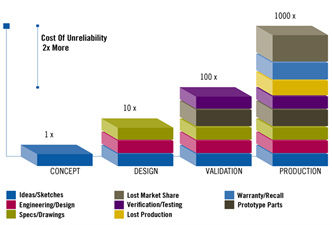
Costs due to reliability and manufacturing
issues can increase by orders of magnitude
the later they are addressed in the design process
- Poor insight into the supply chain.
- The original equipment manufacturer (OEM) requests no feedback on DfM, or has a too-simplistic checklist.
- DfM activities at OEMs are not standardized or distributed.
Design for Manufacturability: Review Best Practices
1. Leverage Industry Standard Design Rules
Leveraging existing industry standards (IPC, JEDEC, ASTM, ISO) when possible is a good starting point for a DfM review. These standards are tried-and-true in many cases. They provide insight into standard design practices and reliability tests for PCBs and PCBAs.
Examples of IPC standards and test methods you can use include:
- IPC-2221- Generic Standard on Printed Board Design
- IPC-A-600 Acceptability of Printed Boards
- IPC-A-610 Acceptability of Electronic Assemblies
- IPC J-STD-001D - Requirements for Soldered Electrical & Electronic Assemblies
- IPC-7095 Design and Assembly Process Implementation for BGAs
- J-STD-020D.01: Joint IPC/JEDEC standard for moisture/reflow sensitivity classification for non- hermetic solid state surface-mount devices
- IPC-TM-650: Test Methods Manual
- Section 1.0: Reporting and Measurement Analysis Methods
- Section 2.1: Visual Test Methods
- Section 2.2: Dimensional Test Methods
- Section 2.3: Chemical Test Methods
- Section 2.4: Mechanical Test Methods
- Section 2.5: Electrical Test Methods
- Section 2.6: Environmental Test Methods
Keep in mind that standards can be backward looking, and it is important to consider additional issues that are specific to your design. Communicate with your suppliers throughout this process. Collaboration is key — you should have representatives from your design, manufacturing, quality, reliability and purchasing teams involved in the DfM process.
2. Conduct a Formal Design Review
The next step in implementing DfM in your workflow is initiating a formal design review. This can be performed by an internal or external team, but the design team performing the review should be insulated from the manufacturer.
A design review evaluates a product, system or application and ensures that each component performs to industry standards. This is a critical step because it ensures you are building an effective product and developing a successful design before prototyping. This conserves business’ resources, reduces cost and, most importantly, expedites time to market.
3. Use Simulation and Design Software
Simulation can be leveraged in certain cases to better understand sources of failure related to manufacturability post reflow. One process that can be evaluated with simulation is in-circuit test (ICT), which is used during PCBA manufacturing to inspect for defects. In some cases, ICT can cause excessive board flexure and lead to component failures.
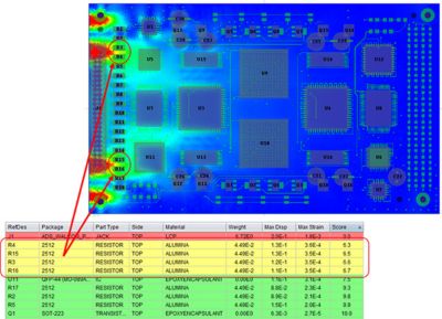
A tool like Ansys Sherlock can perform an in-circuit test analysis to evaluate components at risk of overstress and then quickly compare PCB design or ICT test changes such as adjusting test point locations, reducing test point loads and displacements, or adding or moving board supports to see which components on the board are most at risk during ICT.
Ansys Sherlock analysis determines that 4 resistors on a PCB
are at risk of critical overstress during connector insertion
Another area where simulation can be helpful in the DfM process is in rigid flex technology, which is used to design many consumer electronics like smartphones and laptops that have curved or small form factors. This technology often has more manufacturing steps and it can be difficult to introduce design changes. Simulation can be used in this instance to determine potential failure risks and optimize designs for your desired product.
Trace modeling was recently introduced as a new feature in Sherlock and can be particularly useful for simulating rigid flex technology. This technology allows you to model individual copper traces seen in the various layers of your circuit board. With trace modeling, you actually build the geometry first, then assign materials and a mesh. This is similar to trace mapping available in Ansys Mechanical. Both features are good candidates for capturing small details of your PCB for simulation.
Register for the “Trace Modeling 101” Webinar to learn more.
4. Perform a Materials and Process Audit
Finally, as a last step in the DfM process, it’s important to perform audits of your PCB manufacturers, their contract manufacturers (CMs) and their suppliers — including an onsite audit to review their materials and their process, especially before going through a large production run.
A service like a supplier assessment can evaluate suppliers’ components and technologies to ensure they meet industry standards and confirm your product will not have reliability issues due to manufacturing errors.


