-
-
Kostenlose Software für Studierende
Ansys unterstützt die nächste Generation von Ingenieur*innen
Studenten erhalten kostenlosen Zugang zu erstklassiger Simulationssoftware.
-
Verbinden Sie sich jetzt mit Ansys!
Gestalten Sie Ihre Zukunft
Stellen Sie eine Verbindung mit Ansys her, um zu erfahren, wie Simulation Ihren nächsten Durchbruch vorantreiben kann.
Kostenlose Demoversionen
Produkte & Dienstleistungen
Lernportal
Über das Unternehmen
Back
Produkte & Dienstleistungen
Back
Lernportal
Ansys unterstützt die nächste Generation von Ingenieur*innen
Studenten erhalten kostenlosen Zugang zu erstklassiger Simulationssoftware.
Back
Über das Unternehmen
Gestalten Sie Ihre Zukunft
Stellen Sie eine Verbindung mit Ansys her, um zu erfahren, wie Simulation Ihren nächsten Durchbruch vorantreiben kann.
Kostenlose Demoversionen
ANSYS BLOG
January 25, 2021
Optimize Your PCB for Vibration, Shock and Thermal Environments
When designing printed circuit boards (PCBs), keep in mind the major causes of electronic failure: thermal cycling, vibration, and mechanical shock and drop. You can perform a variety of physical tests to determine how and why electronics fail, however, a much faster and cost-effective solution is PCB modeling and simulation.

When simulation is used in combination with physical testing (i.e., when physical testing is tailored to simulation results and only requires one or two tests), your electronics’ reliability can be virtually guaranteed.
Request an Electronics Reliability Demo using Ansys tools.
PCB Design Optimization for Vibration
When optimizing your PCB design for vibration, the first step is determining the natural frequency range of your PCB. To complete PCB vibration testing, you will need to perform a modal analysis or natural frequency analysis, which can be determined using a vibration simulation tool like Ansys Sherlock or Ansys Mechanical.
Vibration Analysis Example
In the example below, you will see a PCB vibration analysis that has three high-risk components near the bottom of the board where there is strain near the mounting points and larger components. To optimize the design, you can remove the center mounting point and add two mounts, which will relieve strain and resolve one of the component issues.

Figure 2: PCB vibration analysis in Ansys Sherlock.
There are 3 high-risk components (U20, U33, U34)
Next, you can add adhesive staking to the two remaining high-risk components to provide additional component support and alleviate some of the strain.
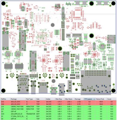
Figure 3: Component U20 issue is resolved by removing the center
mount point and adding two additional mounts
You might also consider moving larger components away from high-strain areas (like mount points, areas between or near large parts, or near V-score breakaways) and keep strain-sensitive components (like BGAs, ceramic capacitors and QFNs) away from high-strain areas. This will ensure your PCB design is optimized for random and harmonic vibration.
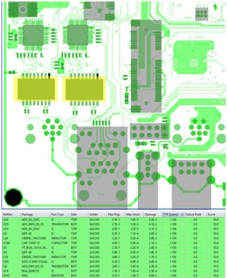
Figure 4: Components U33 and U34 in Figure 2 are resolved by adhesive staking
Watch the “PCBA Design for Shock, Vibration and Thermal Loads” webinar to learn more.
PCB Design Optimization for Shock
Mechanical shock occurs when there is a sudden and irregular acceleration that induces a mechanical displacement. More specifically, it occurs for less than 20 ms with an acceleration of at least 10 G that occurs less than 100,000 times.
A good rule of thumb when designing a PCB for shock is that the resonant frequency of the board should be at least 3X higher than the shock pulse frequency.
Example: 10 ms pulse
- 50 Hz pulse frequency
- Board should be > 150 Hz
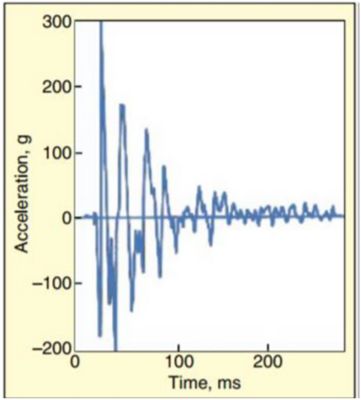
Figure 5: Graph of mechanical
shock acceleration over time
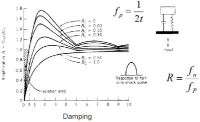
Figure 6: Equation for shock pulse frequency and resonant frequency
For mitigating PCB failure risk from mechanical shock and drop, there are a number of strategies you can use, including:
- Excitation Reduction
Shock isolators (primarily for large electronic assemblies)
External cushioning (cell phone cases, bumpers)
Ejection of mass (battery pops out)
- Component Level
Component selection
Flexible terminations on ceramic capacitors
Leaded parts
Bonding
Underfill/edge-bonding/staking
- PCB Design
PCB thickness
Mount point locations
Talk to one of our reliability experts to learn more about failure analysis.
PCB Design Optimization for Thermal Environments
Temperature cycling is the most common cause of electronic failure. It is typically caused by a coefficient of thermal expansion (CTE) mismatch between the PCB components and the board. The greater the CTE mismatch between the components and the board, the greater the likelihood of solder joint failure.
Download the ”Thermal Management Solutions: How Hot is Too Hot” Whitepaper to learn more.
However, failures can also be caused by localized events. For example, in automotive electronics the PCB is frequently over-constrained within an aluminum housing. The cold side of the PCB will shrink, or the hot side will expand, or both, leading to board buckling.
To analyze for localized events like this, you typically want to run a strain vs. strain comparison, which is an analysis of the board without housing and another analysis of the board inside the housing. This will help determine the increase in the lead strains due to the chassis/enclosure.
PCB Thermal Analysis Example
The example below shows an analysis of a board without a chassis. You can see that the strain is on the BGAs.
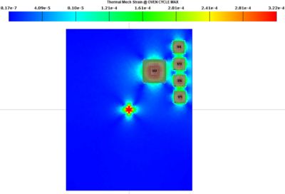
Figure 7: Thermal mechanical analysis of a PCB in Ansys Sherlock (without housing)
We ran an analysis of the board in its housing, where you can see that the strains have doubled.
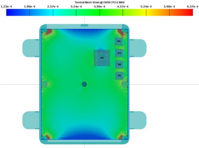
Figure 8: Thermal mechanical analysis of a PCB in Ansys Sherlock (with housing)
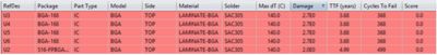
Table 1: Solder fatigue reliability predictions of Figure 9 in Ansys Sherlock
with 5 at-risk components
In Table 1 above, you can see the solder fatigue reliability predictions provided by Sherlock. Having the board mounted in the chassis increases the board’s failure risk. To mitigate these risks, you would need to consider a different chassis material, different PCB mounting points, adhesive staking or other component locations.
As the three examples shared here show, the most important design decisions you can make when designing your board for vibration, shock and thermal environments are:
- Ensuring that strain-sensitive components are removed from high-strain areas.
- Moving your mount points to alleviate stress on the board and components.
- Carefully choosing your materials.
Simulation of each of these environmental factors will reduce test iterations and design times, and provide valuable insight into your product’s reliability and lifetime.