Synopsys and Ansys power the future of innovation—connecting silicon to systems.
-
-
Kostenlose Software für Studierende
Ansys unterstützt die nächste Generation von Ingenieur*innen
Studenten erhalten kostenlosen Zugang zu erstklassiger Simulationssoftware.
-
Verbinden Sie sich jetzt mit Ansys!
Gestalten Sie Ihre Zukunft
Stellen Sie eine Verbindung mit Ansys her, um zu erfahren, wie Simulation Ihren nächsten Durchbruch vorantreiben kann.
Kostenlose Demoversionen
Produkte & Dienstleistungen
Lernportal
Über das Unternehmen
Back
Produkte & Dienstleistungen
Back
Lernportal
Ansys unterstützt die nächste Generation von Ingenieur*innen
Studenten erhalten kostenlosen Zugang zu erstklassiger Simulationssoftware.
Back
Über das Unternehmen
Gestalten Sie Ihre Zukunft
Stellen Sie eine Verbindung mit Ansys her, um zu erfahren, wie Simulation Ihren nächsten Durchbruch vorantreiben kann.
Kostenlose Demoversionen
ANSYS BLOG
April 27, 2021
Wired for Success: Ansys HFSS Leads in Wirebond Simulation
As semiconductor manufacturers face increasing demand for faster processing speeds, all components of the printed circuit board (PCB) and chip package must deliver uncompromising signal integrity at ultra-fast data rates. Any design aspects that could potentially cause discontinuities and unwanted signal coupling must be painstakingly tested for defects.
Wirebonds — the microscopic “stitches” that connect chips and substrates within a PCB or chip package — are under special scrutiny. Because they represent connection points, they are often the source of signal loss or degradation. Semiconductor engineering teams must design wirebonds for extreme reliability, considering everything from their material and their bonding parameters to the environmental operating conditions.
Speed is of the essence in analyzing potential wirebond designs and accurately predicting their performance as part of a PCB or chip package. Budgets, staff hours and other resources needed for exhaustive physical testing are limited. How can electronics engineers achieve the level of analytic rigor needed to deliver flawless wirebond performance, while also meeting ambitious launch deadlines and financial objectives?
Unmatched Capabilities for Wirebond Simulation
The answer lies in modeling wirebonds and simulating their performance — along with every other aspect of PCBs and chip packages — via Ansys HFSS.
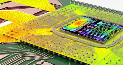
Ansys offers a complete simulation environment for modeling chip, package, printed circuit board (PCB) and the entire system.
HFSS is the industry standard for the simulation of high-frequency signal and power integrity designs, offering native support for drawing, importing and modifying wirebond structures. No matter how demanding the design requirements, this hardworking solution enables engineers to solve complex challenges like materials selection and thickness, package configuration and bonding parameters with ease.
Now there are additional capabilities in Ansys Electronics Desktop with HFSS 3D Layout 2021 R1, including a powerful new wirebond editing platform and library management function. Engineering teams can develop and share their own custom libraries of wirebond profiles, so they don’t have to start from scratch with each new product design. This saves both time and money as product developers rush to market with new designs.
The Ansys wirebond library also supports seamless importing of Cadence wirebond profiles, as well as the ability to store them for future use.
The Only End-to-End Solution for Semiconductor Development
By relying on HFSS, engineers can simulate not only the chip design, but its level of signal and power integrity when exposed to different use environments.
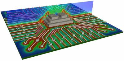
Ansys solutions are capable of modeling single, multiple and 3DIC structures, including wirebonds and complex interconnects.
Once wirebonds have been optimized for electrical performance via HFSS, they can be optimized for other physical characteristics such as thermal and structural reliability in a straightforward, streamlined process. The Ansys simulation platform, which includes both HFSS and Ansys Mechanical, provides the only single-source environment for verifying all aspects, electromagnetics, thermal and structural, of PCB and chip package design, including wirebonds.
Today’s smaller, denser electronics package designs have a higher risk of thermal or structural failures when they’re exposed to demanding real-world conditions. As a microscopic connection point, wirebonds must be subjected to especially rigorous failure analysis. Ansys makes it easy and fast to hand off wirebond designs to Mechanical for this analysis ― then they can be sent back to Ansys HFSS for iterative design.
With HFSS, semiconductor engineering teams can not only ensure that individual components, such as wirebonds, are optimized for real-world conditions ― but they can also ensure that the entire system works together in an optimal, reliable manner after it is assembled and exposed to harsh operating conditions.
The world’s semiconductor leaders are leveraging Ansys solutions to achieve speedups of 10x to 12x in their electromagnetic simulation run times for complex products. This system-level approach, along with industry-leading capabilities for specific tasks such as wirebond optimization, capitalize on more than 50 years of Ansys industry leadership.
Bond with Ansys Today
As the job of semiconductor engineering has become more complex, HFSS has consistently evolved to meet new challenges. HFSS capabilities for wirebond modeling and simulation are no exception. Ansys HFSS 2021 R2, scheduled for release this summer, promises even more game-changing enhancements that anticipate and address the most urgent needs of semiconductor engineering teams.
Ready to explore the significant benefits of applying HFSS for wirebond modeling and simulation? Check out the many HFSS on-demand educational courses at the online Ansys Training Center, or register attend Simulation World 2021, the annual Ansys user conference that was held virtually April 20-22 and is still available on demand for a limited time.