-
-
Kostenlose Software für Studierende
Ansys unterstützt die nächste Generation von Ingenieur*innen
Studenten erhalten kostenlosen Zugang zu erstklassiger Simulationssoftware.
-
Verbinden Sie sich jetzt mit Ansys!
Gestalten Sie Ihre Zukunft
Stellen Sie eine Verbindung mit Ansys her, um zu erfahren, wie Simulation Ihren nächsten Durchbruch vorantreiben kann.
Länder und Regionen
Kostenlose Demoversionen
Produkte & Dienstleistungen
Lernportal
Über das Unternehmen
Back
Produkte & Dienstleistungen
Back
Lernportal
Ansys unterstützt die nächste Generation von Ingenieur*innen
Studenten erhalten kostenlosen Zugang zu erstklassiger Simulationssoftware.
Back
Über das Unternehmen
Gestalten Sie Ihre Zukunft
Stellen Sie eine Verbindung mit Ansys her, um zu erfahren, wie Simulation Ihren nächsten Durchbruch vorantreiben kann.
Kostenlose Demoversionen
ANSYS BLOG
November 30, 2017
Ensuring EMI/EMC Compliance with Electronics Simulation
Today we live in a hyper-connected world, surrounded by smart products. If industry forecasts are correct, by 2020 — just 2 short years from now — there will be over 28 billion internet-connected devices. Beyond smart phones and autonomous vehicles, smart cities, smart factories, and smart homes are also quickly emerging as promising opportunities that could help improve how we live, work and play.
While these new capabilities will be a delight to us as consumers, they are a nightmare for engineers and product designers. With hundreds of sensors, microprocessors, and wired and wireless communication components, engineers face immense challenges in ensuring reliability and performance. In the complex web of electronic circuitry, something, somewhere that is left unaddressed could lead to failure. One of the big challenges confronting product designers is electromagnetic interference, or EMI.
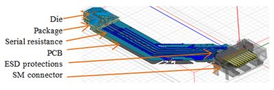
Full-wave model of communications channel
A product that creates electromagnetic interference could not only malfunction itself, but could also cause other electronic devices to malfunction. EMI and electromagnetic compatibility (EMC) standards exist to ensure that this does not happen, but it is becoming increasing difficult to meet them due to the proliferation of electronics operating at higher data rates and package densities. Each added interface has the potential to interfere electromagnetically with an existing one, leading to the degradation of communications in one or both. Fortunately, Ansys electronic simulations make it possible to detect potential EMI/EMC problems early in the design stage of ICs and PCBs, when design changes are easier and less costly to make.
STMicroelectronics Tackles EMI
Engineers at STMicroelectronics, a global semiconductor company with solutions for autonomous vehicles and the Internet of Things, have combined the Ansys HFSS full-wave simulation with HFSS circuit simulation through the Ansys Electronics Desktop to produce a streamlined workflow that has cut their normal product development time by 20 percent.
Ansys HFSS 3D electromagnetic solution delivers 3D full-wave accuracy for components in a broad range of applications including antennas, phased arrays, passive RF/mW components, high-speed interconnects, connectors, IC packaging and PCBs. When this full-wave solution is combined with HFSS circuit simulation and high-performance computing (HPC) capabilities, EMI/EMC-compliant electronic devices can be designed, tested and validated in record time. Ansys Electronics Desktop is a unified, easy-to-use design platform for electromagnetic, circuit and system simulation.
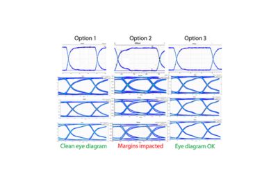
Eye diagrams of the clock with common mode filtering used at three different locations
The method developed by STMicroelectronics engineers performs transient simulation using the full-wave model with realistic excitation patterns, which generates eye diagrams and H-fields. The excitation of the circuit simulation is then fed back into the HFSS full-wave model to recalculate real-world electromagnetic fields.
Combining this new method with HPC, the engineers were able to quickly analyze the high-speed digital transmission channels of a set-top box to ensure EMI/EMC compatibility.