Synopsys and Ansys power the future of innovation—connecting silicon to systems.
-
-
Access Free Student Software
Ansys empowers the next generation of engineers
Students get free access to world-class simulation software.
-
Connect with Ansys Now!
Design your future
Connect with Ansys to explore how simulation can power your next breakthrough.
Free Trials
Products & Services
Learn
About
Back
Products & Services
Back
Learn
Ansys empowers the next generation of engineers
Students get free access to world-class simulation software.
Back
About
Design your future
Connect with Ansys to explore how simulation can power your next breakthrough.
Free Trials
TOPIC DETAILS
What is a MicroLED?
Optics and photonics technologies are rapidly evolving in display applications. OLED TVs are currently the biggest commercial market, but microLEDs are considered the next generation of LED displays due to better response times, lower power consumption, greater energy efficiency, and higher resolution.
What is MicroLED Technology?
MicroLEDs (μLEDs) are micrometer-sized devices made from III-V compounds — elements on the third and fifth columns of the periodic table — such as indium gallium nitride (InGaN) and aluminum gallium indium phosphide (AlGaInP). MicroLEDs are small, flat, square light sources that can be built into arrays with a very high contrast. Each LED in a microLED display acts as a pixel (either red, green, or blue) and can be used in microLED TVs and other technologies requiring advanced displays.
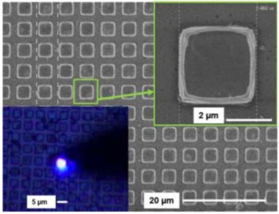
Flat and square LEDs
MicroLEDs work differently from LCD-based displays. Traditional LCD systems use an LED backlight and a liquid crystal layer that creates images by blocking certain parts of the light. In contrast, both microLED and OLED displays are much simpler because they do not rely on LCDs. Instead, each LED emits its own light, creating the image from each individual pixel.
How Are MicroLEDs Manufactured?
In an ideal scenario, epitaxial growth, or growing the LEDs directly on the backplane, via monolithic integration would be the best fabrication route for microLEDs. This is currently a work-in-progress area in which companies are developing prototype strategies, but the current costs to perform these methods are too expensive to be commercially feasible.
Today, microLEDs are more commonly fabricated using the pick-and-place transfer method. In this approach, the red, green, and blue LEDs are fabricated directly onto a wafer and then individually transferred to the backplane, which contains a substrate and the electronic parts needed to control the light. The mass transfer process needs to be fast, precise, and reliable to ensure all the LEDs are properly aligned on the backplane.
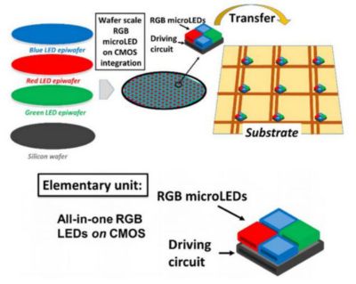
The pick-and-place transfer process
Despite the challenges in large-scale manufacturing, LG, Sony, and Samsung are developing large, premium microLED TVs. Still, many design and scale challenges need to be addressed before they become available to the average consumer. At the moment, these TVs are very expensive due to the time-consuming and costly pick-and-place fabrication process.
Design Challenges of Manufacturing MicroLEDs
MicroLED technology is not yet mature, and designers can employ many different semiconductor fabrication methods in the manufacturing process. Some key considerations for developers in microLED design include:
- Incoherent emission at the macroscopic level in large pixel arrays. To avoid this, designers can use other optical elements such as filters, lenses, color conversion layers, scattering structures, polarizers, and gratings to improve the color definition of the display.
- Stricter tolerance requirements at smaller LED sizes. Tolerance for dimension changes and misalignment becomes more stringent for small LEDs, especially at increased pixel densities.
- Atomic-scale defects and imperfections at the edges of an LED, which can reduce the internal efficiency of the device.
- Increased demand for highly compact, power-efficient, and complex thin film transistor (TFT) drivers to accommodate shrinking subpixel sizes. Subpixels contain the RGB elements needed to create color in displays, so TFTs must control each pixel quickly and precisely.
- Avoiding defects that can arise at any stage of production. Even fabrication processes can still generate dead pixels that must be accounted for.
How Do MicroLEDs Compare to Other LED Technology?
OLED displays and OLED technology have become the gold standard in recent years, but how do they compare to microLEDs? There are many different metrics for measuring OLED, microLED, LCD, and mini-LED performance. Overall, the simpler structure of microLED technology generates a higher-quality image because it has a higher contrast ratio and faster response time. MicroLED displays can also be made flexible like OLED displays.
MicroLEDs stand out from other LED technologies through:
- Smaller and brighter pixels with an improved color gamut. MicroLEDs have a luminance of more than 100,000 nits compared to 500-1,000 nits for OLEDs and 3,000 nits for LCDs. Some microLED displays can reach luminance levels of more than 250,000 nits. Higher luminance does not cause efficiency roll-off, aging, or adverse thermal effects.
- Around 10% theoretical external quantum efficiency (EQE) improvements over OLEDs
- Longer lifetimes, as inorganic materials produce long-lasting LEDs compared to organic materials
- Resistance to oxidation and other environmental effects
- A wider operating temperature range (-100 to 120 °C)
- Better visibility in sunlight and more viewing angles
- Quick response times on the order of nanoseconds compared to microseconds or milliseconds
- The potential (in blue LEDs) to become the excitation source for the quantum dots inside QLED TVs
What Are the Applications of MicroLEDs?
Despite not being commercially mature, the extra performance increase over other LED technologies ― especially in terms of brightness, flexibility, picture quality, and longevity ― has opened microLEDs to a range of advanced display technologies. Some key examples of microLEDs use include:
- Wearable technology, such as smart watches and fitness bands
- MicroLED TVs
- Augmented/virtual reality (AR/VR) glasses and headsets
- Heads-up displays (HUDs) in the automotive and aerospace industries
- Central cluster displays
- Automotive headlights
- High-speed light-based communications
- Flexible and stretchable displays
Simulating MicroLEDs With Ansys
Engineers can overcome the many design challenges in microLEDs by first using simulation methods to visualize how the LED or display will behave. Ansys has a range of tools available for simulating the performance of microLEDs before physical fabrication takes place:
Ansys Lumerical STACK solver: simulates the different material layers in microLEDs to show how light is reflected, refracted, and transmitted through them. The STACK solver also calculates the emitted power and power density of LEDs.
Ansy Lumerical FDTD solver: simulates far-field emission patterns and extraction efficiency of LEDs. The FDTD solver also computes the spectral intensity in conoscopic coordinates for use with Ansys Speos design tools.
Ansys Lumerical CHARGE and Ansys Lumerical MQW solvers: simulate the current-voltage (I-V) curve, spontaneous emission power spectrum, and internal quantum efficiency of LEDs.
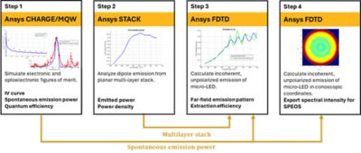
Workflow overview for Ansys Lumerical solvers
Ansys Speos software: performs system-level simulations using spectral intensity data from Lumerical suite solvers and acts as a virtual photometric lab. It enables engineers to examine the full color gamut and perform radiometric testing.
Discover how you can overcome design challenges in microLED technology before undergoing the complex fabrication process by contacting our technical team.
Related Resources
Let’s Get Started
If you're facing engineering challenges, our team is here to assist. With a wealth of experience and a commitment to innovation, we invite you to reach out to us. Let's collaborate to turn your engineering obstacles into opportunities for growth and success. Contact us today to start the conversation.