Synopsys and Ansys power the future of innovation—connecting silicon to systems.
什么是MicroLED?
光学和光子学技术在显示应用中迅速发展。OLED电视是目前最大的商业市场之一,但MicroLED凭借更快的响应时间、更低的功耗、更高的能效和分辨率,被视为下一代LED显示器。
什么是MicroLED技术?
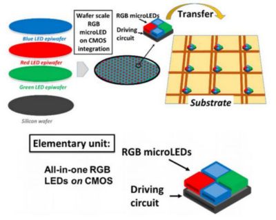
MicroLED(μLED)是由氮化铟镓(InGaN)和磷化铝镓铟(AlGaInP)等III-V族化合物(位于元素周期表第三列和第五列)制成的微米级器件。MicroLED是小型、扁平、方形的光源,可以内置在具有极高对比度的阵列中。MicroLED显示器中的每个LED都可充当一个像素(红色、绿色或蓝色),可用于MicroLED电视和其他需要高级显示器的技术。
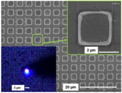
扁平、方形的LED
MicroLED显示器的工作原理与基于LCD的显示器不同。传统的LCD系统使用LED背光和液晶层,后者通过阻挡某些部分的光来创建图像。相比之下,MicroLED和OLED显示器都要简单得多,因为它们不依赖LCD。相反,每个LED都会自己发射光,从而从每个单独的像素创建图像。
MicroLED是如何制造的?
拾放式转移方法流程
尽管大规模制造存在一些挑战,LG、索尼和三星等企业仍在开发大型高端MicroLED电视。当然,在它们面向消费者推出之前,仍需要解决许多设计和规模挑战。目前,由于耗时且成本高昂的拾放式制造流程,这些电视的成本非常高昂。
MicroLED制造面临的设计挑战
MicroLED技术尚未成熟,设计人员可以在制造流程中采用许多不同的半导体制造方法。开发人员在MicroLED设计中的一些关键考虑因素包括:
- 大规模像素阵列在宏观层面的非相干发射。为了避免这种情况,设计人员可以使用滤光片、透镜、颜色转换层、散射结构、偏光片和光栅等其他光学元件来改进显示器的颜色定义。
- 小尺寸LED具有更严格的公差要求。尺寸变化和未对齐的公差对于小型LED来说变得更加严格,尤其是在像素密度增加的情况下。
- 如果LED边缘存在原子尺度缺陷和结构不完善,会导致器件内部效率下降。
- 为了适应不断缩小的子像素尺寸,对高度紧凑、节能且复杂的薄膜晶体管(TFT)驱动器的需求正在增加。子像素包含了在显示器中创建颜色所需的RGB元素,因此TFT必须快速准确地控制每个像素,
- 以避免在生产的任何阶段可能出现的缺陷。即使是制造过程本身,也仍然可能产生死像素,因此必须对这些问题加以考虑。
MicroLED与其他LED技术有何不同?
近年来,OLED显示器和OLED技术已成为黄金标准,但它们与MicroLED有何不同?有许多不同的指标可用于衡量OLED、MicroLED、LCD和mini-LED性能。总体来说,MicroLED技术的结构更简单,可生成更高质量的图像,因为它具有更高的对比度和更快的响应时间。此外,MicroLED显示器也可以像OLED显示器一样制作成柔性的。
MicroLED凭借以下优势,从其他LED技术中脱颖而出:
- 更小、更明亮的像素,具有改进的色域。MicroLED的亮度超过100,000 nits,而OLED的亮度为500-1,000 nits,LCD的亮度为3,000 nits。一些MicroLED显示器的亮度级可能超过250,000 nits。更高的亮度不会导致效率下降、老化或不利的热效应。
- 从理论上说,其外量子效率(EQE)比OLED提高了10%左右
- 使用寿命更长,因为无机材料制成的LED相较于有机材料制成的LED更具耐久性。
- 抗氧化和其他环境影响
- 更宽的工作温度范围(-100至120°C)
- 在阳光下更好的可见性和更广的可视角度
- 纳秒级的快速响应时间,而其他显示器的响应时间为微秒或毫秒级
- MicroLED(在蓝光LED应用方面)有望成为QLED电视内部量子点发光的光源
MicroLED有哪些应用?
尽管MicroLED尚未达到商业成熟阶段,但其相较于其他LED技术在亮度、柔性、图像质量及使用寿命等方面的显著性能提升,已使其得以应用于多种先进显示技术领域。一些主要的MicroLED使用示例包括:
- 智能手表和健身手环等可穿戴技术
- MicroLED电视
- 增强/虚拟现实(AR/VR)眼镜和耳机
- 汽车和航空航天行业的抬头显示器(HUD)
- 中央集群显示器
- 汽车前照灯
- 高速光通信
- 柔性可拉伸的显示器
使用Ansys进行MicroLED仿真
工程师可以首先通过仿真方法来可视化LED或显示器的工作表现,以克服MicroLED中的诸多设计挑战。Ansys提供了一系列工具,可用于在进行物理制造之前对MicroLED性能进行仿真:
Ansys Lumerical STACK求解器:对MicroLED中的不同材料层进行仿真,以显示光是如何反射、折射和透射的。STACK求解器还可计算LED的发射功率和功率密度。
Ansy Lumerical FDTD求解器:对LED的远场发射方向图和提取效率进行仿真。FDTD求解器还可以与Ansys Speos设计工具配合使用,计算锥光坐标中的光谱强度。
Ansys Lumerical CHARGE和Ansys Lumerical MQW求解器:对LED的电流-电压(I-V)曲线、自发发射功率频谱和内部量子效率进行仿真。
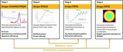
Ansys Lumerical求解器工作流程概览
Ansys Speos软件:使用来自Lumerical套件求解器的光谱强度数据执行系统级仿真,并充当虚拟光度实验室。利用该工具,工程师可以检查全色域并执行辐射测试。
欢迎联系我们的技术团队,了解如何在进行复杂的制造流程之前克服MicroLED技术中的设计挑战。
相关资源
现在就开始行动吧!
如果您面临工程方面的挑战,我们的团队将随时为您提供帮助。我们拥有丰富的经验并秉持创新承诺,期待与您联系。让我们携手合作,将您的工程挑战转化为价值增长和成功的机遇。欢迎立即联系我们进行交流。