Skip to Main Content
Countries & Regions

Synopsys and Ansys power the future of innovation—connecting silicon to systems.

Design Exploration of RF GaN Amplifier, 3D Packaging, and Thermal Analysis

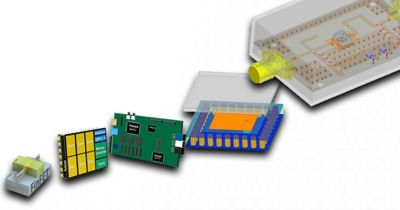
Join us for this webinar on RF GaN amplifier design using electromagnetic/thermal 3D solvers. We will discuss the step-by-step process of building a GaN amplifier, beginning with the transistor model in the circuit simulator. The webinar will outline the steps required to convert this to a physical layout for electromagnetic simulation and verification while integrating packaging and thermal effects co-simulation to analyze a complete packaged system. Discover how this comprehensive approach yields innovative solutions, important design insights, and their potential impact on packaged performance.

Venue:
Digital
Watch Presentation

This site is protected by reCAPTCHA and the Google Privacy Policy and Terms of Service apply.

What You Will Learn

  • Design and layout of a typical GaN amplifier using circuit
    and 3D EM tools
  • Incorporation of 3D component models (connectors, packages etc) for complete system analysis
  • Co-simulation of packaged devices with thermal solvers

Who Should Attend

  • Electromagnetic and circuit design engineers: Delve into the co-
    simulation nuances between circuit models and full 3D designs
  • System engineers: Develop an understanding of the packaged PA design and tradeoffs
  • Professionals in wireless communication: Gain comprehensive
    insights into the modern circuit/package co-simulation
    workflows

Speaker

David Edgar, Senior Manager Applications Engineer

2023-5g-workflow-webpage.jpg