Case Study
-
-
Access Free Student Software
Ansys empowers the next generation of engineers
Students get free access to world-class simulation software.
-
Connect with Ansys Now!
Design your future
Connect with Ansys to explore how simulation can power your next breakthrough.
Countries & Regions
Free Trials
Products & Services
Learn
About
Back
Products & Services
Back
Learn
Ansys empowers the next generation of engineers
Students get free access to world-class simulation software.
Back
About
Design your future
Connect with Ansys to explore how simulation can power your next breakthrough.
Free Trials
“What I believe fundamentally is that what Ansys simulation does — and has always done for us — is not only reduce the development time but also reduce the number of required prototypes. If you can plan your experiments — if you can develop models that give you a better idea of the experiments you should run — it’s possible to realize a 25-30% reduction across your development cycles.”
- Russ Robison, Technical Lead, EDA/ODK Strategy / IBM Research
In an IBM Research lab in Albany, New York, researchers are busy designing electronic devices supporting innovations that will dramatically change how we all live in the future, from the personal electronics we use to the vehicles we drive. Due to recent investments in technology, including the cHIPS and Science Act in the United States, the semiconductor ecosystem has exploded with new ideas. New developments, including IBM Research's gate-all-around (GAA) transistor technology, are cascading into new opportunities, resulting in new challenges. These include how to apply this technology in new and different ways, as well as how to innovate around them in a fast-paced environment with a finite number of dollars and people available to do the work.
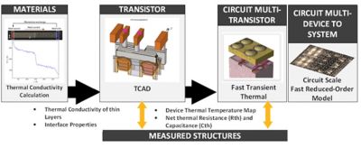
Figure 1. Illustration of the process to capture both atomistic properties, single-device behaviors, and circuit thermal aspects in a multiscale flow
Challenges
The semiconductor industry is constantly evolving in the advancement and adoption of increasingly complex designs. Aggressively scaled technology nodes along with the critically small dimensions of these new chips create thermal management issues as a function of power density imbalances between the transistor and the device area. The short channel length of these nanosheet transistor architectures, while improving performance, are prone to thermal instability and leakage current. Overcoming these challenges requires an understanding of material structural characteristics impacting thermal behavior on an atomic scale.
To counter these challenges and others, multiple variations of a design must be assessed for thermal and mechanical integrity. Thermal finite element simulations can be limited by computational resources, like memory and processor speed, that limit the number of static and transient simulations that can be performed, and the ability to scale in design complexity.
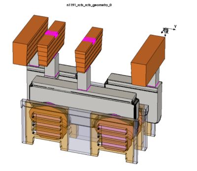
Figure 2. Example inverter cell layout created in Sentaurus TcAD flow
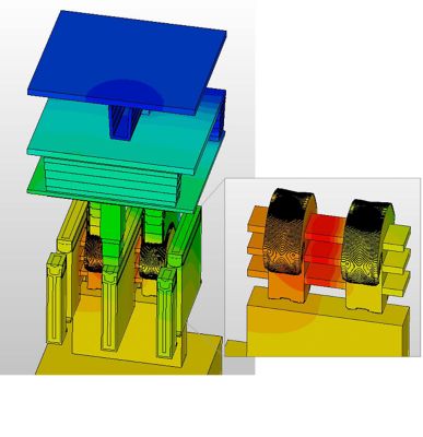
Figure 3. Example inverter cell layout created in Sentaurus TcAD flow post-process
This requires additional resources (departments) on the design side to model each variation and understand just where the holes are. Therefore, IBM Research must continuously scale up to embrace an increasing level of complexity with a containable number of resources.
"It’s a challenge, fundamentally, that none of these things ever look like you think they do on paper,” says Russ Robison, technical lead for EDA/PDK Strategy at IBM Research. “Our team is constantly looking at experimental results that, on the surface, simply do not make sense. One of the key things that we use virtual modeling for is to understand, in fact, if what we're getting is truly valid or not.”
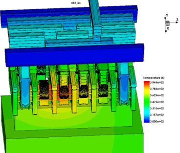
Figure 4. Thermal simulation of a fully realized multisheet, multigate GAA standard cell device
Engineering Solutions
Ansys has been engaged with IBM Research on semiconductor development for several years in the use of simulation to assess power integrity, as well as generalized simulation of the stress, strain, and thermal behaviors of IBM Research's GAA technology. This includes a novel thermal workflow that leverages Ansys tools and solvers to capture thermal effects during circuit-level interactions and arrive at single-device measurements supporting large-scale circuit validation.
Working through digital models with the broader team enables Robison to arrive at a more realistic understanding around expected thermal behavior of a device, or what the actual measurement or test should be showing within the context of a particular design concept. With the help of Ansys simulation software, it's then possible move past initial assumptions of what the data might look like to arrive at novel solutions.
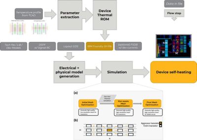
Figure 5. Example circuit-level workflow block diagram utilizing TcAD input and circuit design and layout. Inset: (a) Thermal simulation workflow; (b) schematic showing aggressor and victim for thermal simulation
In one instance, with the help of advanced machine learning algorithms, IBM Research could produce a highly accurate reduced order model (ROM) trained against 512 finite element simulations within an hour. It involves training data generated using finite element analysis across user-definable NxN subsections and tiles, and a single tile heating power map to generate the heating thermal profile (output) post-processed using linear superposition of thermal responses.
The resulting transistor-level ROM was then applied to a ring oscillator circuit simulation (~1000 transistors) and achieved a high correlation between simulation and measurement.
To further illustrate the ability of this methodology to scale in design complexity (pictured above), a SAIL-latch system was analyzed and achieved 50,000x greater speed beyond existing simulations with <1.0C accuracy.
“The internal feedback from the team is that Ansys is the only answer they trust,” says Robison. “Even if another tool is involved, Ansys will be the tool it’s compared to. It's a gold standard for us. It doesn’t feel like Ansys just sells a software tool. They literally sell success.”
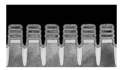
Figure 6. Cross-sectional TEM of IBM Research’s gate-all-around nanosheet transistor architecture
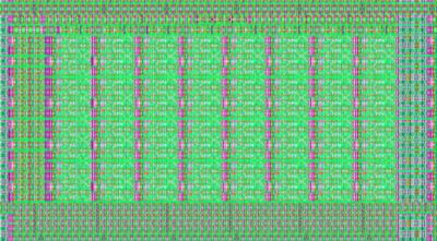
Figure 7. Example of a six-transistor (6T) SrAM bitcell that will be used for electrical validation of the simulation workflow. Thousands of these cells comprise the key thermal validation circuit.
Benefits
- IBM Research uses Ansys multiphysics tools and solvers to continually evaluate what the results of an experiment should be and ascertain if what it is getting is valid or not.
- Ansys simulation software played an integral role in the implementation of a multiscale, multitool workflow to address thermal-related scalability challenges during the design phase.
- Using the new workflow, it was possible to model the static and transient thermal behavior of design structures to pinpoint reliability risks as a function of the material, transistor, and circuit involved.
- Specifically, the atomic-scale simulation of the thin layer surfaces and surrounding interfaces of semiconductor design enabled the more accurate description of thermal behavior to the electrical resistance characteristics of a device.
- Combining extracted thermal conductivities from atomistic simulation with accurate structural and electrical modeling facilitated confident modeling of measured hardware results and temperature behavior of IBM Research's GAA technology.
- In providing a multiscale simulation framework to benchmark thermal behavior of its GAA transistors, IBM Research created a full-stack pathway to optimize next-generation nanosheet technology performance apart from any resource restrictions related to people, time, and cost.
Let’s Get Started
If you're facing engineering challenges, our team is here to assist. With a wealth of experience and a commitment to innovation, we invite you to reach out to us. Let's collaborate to turn your engineering obstacles into opportunities for growth and success. Contact us today to start the conversation.