ANSYS BLOG
September 26, 2023
Join Ansys at TSMC Open Innovation Platform 2023
Every year, TSMC brings together its customers and the semiconductor design community for the TSMC Open Innovation Platform® (OIP) event in Silicon Valley to effectively promote innovation in the semiconductor industry. This is an ideal platform to discuss the latest technologies and design solutions for high-performance computing (HPC), artificial intelligence/machine learning (AI/ML), mobile, automotive, and internet of things (IoT) applications.
Ansys participates in TSMC-OIP as one of the big-four electronic design automation (EDA) companies and a key signoff technology provider for power integrity verification and 3D-IC multiphysics analysis. Ansys provides a broad range of multiphysics analysis tools that have become increasingly central for advanced semiconductor manufacturing and are currently used by the large majority of integrated circuit (IC) design teams in the world. Traditional signoff analyses like voltage drop and electromigration (EM/IR) have become more acute at 2nm and 3nm as transistor architectures grow more complex, as design sizes grow larger, and as ultra-low supply voltages lead to vanishing safety margins. Ansys and Iluvatar Core X® are presenting a joint paper on “A Novel Methodology for GP-GPU Power Delivery Network Design to Improve Power and Performance” at OIP China on recent development is power integrity signoff for HPC.
Realize the Advantages of 3D Fabric
Beyond this traditional Moore’s Law scaling, TSMC has also developed its 3DFabric technologies for 2.5D/3D-IC multi-die heterogeneous integration, which assembles multiple bare chips into a small package. This multi-die technology has been adopted by all the leading semiconductor companies for HPC design because it provides unparalleled system integration, performance, and reduced power. But with all these advantages come a series of novel design challenges that stem from multiphysics interactions that blur the lines between chip, package, and board design. Ansys has vast experience with these multiphysics effects — like thermal integrity, electromagnetic signal integrity, and structural reliability — that it has been able to provide to 3D-IC designers with solutions like Ansys RaptorX and Ansys RedHawk-SC Electrothermal. But the complexity of 3D-IC is such that no single company can offer all the design technology required to realize the advantages of 3DFabric. To make 3D-IC design easier, TSMC has developed the 3Dblox™ reference flow and language standard that enables 3D-IC design data to be easily and transparently exchanged between multiple tools. Ansys multiphysics signoff solutions for 3D-IC including Ansys RedHawk-SC, RedHawk-SC Electrothermal, and Ansys Totem fully support the 3Dblox language. This new capability is described in the OIP paper on: “3DIC Multiphysics Simulation Technologies Enabled by Ansys RedHawk-SC, RedHawk-SC Electrothermal and TSMC 3Dblox.”
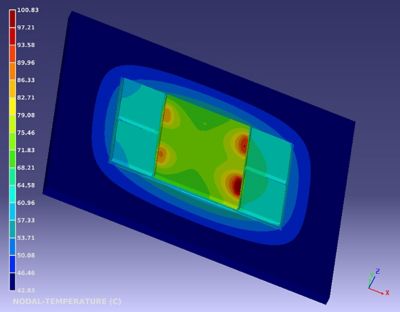
Simulate Thermal Phenomena
One of the most urgent issues facing 2.5D and 3D-IC designers is thermal signoff. Thermal heating is the No. 1 limiting factor of achievable integration density today. Early thermal planning is crucial to avoid placing hot chips too closely together. But thermal analysis is vitally dependent on realistic activity vectors that need to be much longer than traditional timing vectors. This is because the time constants that govern thermal spreading are so much slower than electrical time constants. Ansys PowerArtist is a register transfer level (RTL) power analysis and reduction tool that also has links to hardware emulators to stream ultra-long activity vectors needed for thermal analysis.
Optimize High-Frequency Design
TSMC has also developed a new generation of silicon technologies optimized for radio frequency (RF) and millimeter-wave (mmWave) design. Ansys has collaborated with TSMC and OIP partner companies Synopsys and Keysight to develop integrated RF Reference Flows that provide complete mmWave EDA solutions for TSMC customers. More details on these high-frequency design capabilities will be explained in “Synopsys/Ansys/Keysight RF Reference Design Flow on TSMC Advanced N4P Process” jointly presented by all three partners.
Optical communication and co-packaged optics are another form of high-frequency design that has been gaining wide acceptance as the low-latency solution for datacenter communication backplanes. Ansys technology provides optical solvers for the entire range of optical effects — from the semiconductor device level, to lens-based systems, all the way to human perception simulation. Advances in optical design are highlighted at TSMC OIP by Ansys’ photonics group in “Advancing Co-Packaged Optics: Towards a Comprehensive Solution for Optical System Design.”
Come join us at TSMC OIP on September 27 at the Santa Clara Convention Center in Silicon Valley. Visit the Ansys booth to speak with experts and learn about the latest design technologies and what is coming next. For more information visit TSMC OIP and the Ansys Semiconductor web pages.