Synopsys and Ansys power the future of innovation—connecting silicon to systems.
-
-
Access Free Student Software
Ansys empowers the next generation of engineers
Students get free access to world-class simulation software.
-
Connect with Ansys Now!
Design your future
Connect with Ansys to explore how simulation can power your next breakthrough.
Free Trials
Products & Services
Learn
About
Back
Products & Services
Back
Learn
Ansys empowers the next generation of engineers
Students get free access to world-class simulation software.
Back
About
Design your future
Connect with Ansys to explore how simulation can power your next breakthrough.
Free Trials
TOPIC DETAILS
What Is a CMOS Image Sensor?
A CMOS image sensor is a semiconductor device with complementary metal oxide semiconductor (CMOS) technology designed to turn incoming light into a digital image. Like most digital cameras, it detects incoming light with thousands of photon detectors on the surface of a semiconductor chip. Each detector measures the frequency (color) and count (brightness) of photons absorbed by converting the energy of the photons into an electrical current. That current is then amplified by transistors attached to each detector. This type of image sensor is called an active-pixel sensor (APS).
Because CMOS image sensors are constructed with standard semiconductor manufacturing technology, the chips usually include signal processing, analog-to-digital converter, and digital logic on-chip. This results in a full camera on a chip. This technology has enabled many imaging applications, including tiny digital cameras on smartphones, high-definition, high-speed professional video cameras, and Earth observation sensors on satellites.
CMOS vs CCD Image Sensors
The two dominant image sensor technologies, charge couple devices (CCD) and CMOS sensors, were developed at the same time in the late 1960s. Both leverage the photoelectric effect, which occurs when a particle of light,[1] a photon is absorbed into an atom and imparts energy to the electrons in the atom.
If enough energy is absorbed, the atom ejects electrons, creating a negative charge in the semiconductor material. The light-absorbing, electron-producing area of an image sensor is called a photodiode. The photodiodes are arranged into an array that can measure the color and intensity of light focused on their surface.
In CCD sensors, the electrons from the photodiode are captured into a series of capacitors and then amplified. In a CMOS sensor, the electrons are fed directly into transistors and amplified at the detector. The big advantage of the CCD approach is that the capacitors are behind the photodiode, giving a larger light-absorbing area for each pixel. The transistors in a CMOS sensor are next to the photodiode, leaving as little as 30% of the surface area, called the fill factor, for light detection.
CMOS technology is a well-established semiconductor manufacturing process, so CMOS sensors are much less expensive to manufacture than CCD cameras. Initially, CCD sensors were used more often because they produced higher-quality images with less noise, while CMOS sensors were utilized when a more power-efficient or less expensive solution was needed.
Over time, improvements in semiconductor manufacturing technology allowed the pixel size in a CMOS image sensor to be smaller, and on-chip digital signal processing could address the quality issues. These improvements brought image quality on par with CCD sensors while keeping the advantages of lower cost and greater energy efficiency. As such, low-power, high-resolution CMOS image sensors became the preferred choice for most applications by the late 2010s.
Today, CCD devices are primarily used in high-end applications that require low noise and greater sensitivity, such as photo-astronomy, machine vision systems, and microscope cameras. However, CMOS image sensors are also making their way into those applications.
CCD and CMOS Technology Compared
| CCD | CMOS |
Approach | Cascading Capacitors | Photodiode connected to transistors |
Detector Signal Type | Electron Packets | Voltage |
Chip Output | Analog Signal | Digital |
Image Quality | High | Moderate to High |
Power Consumption | Moderate to High | Low |
Cost | Moderate | Low at Volume |
Speed | Moderate | High |
Dynamic Range | High | Moderate |
Quantum Efficiency | High | Moderate to High |
The Geometry of a CMOS Image Sensor
CMOS image sensors are made of an array of pixels, with each pixel captured by four photodetectors, one for red, one for blue, and two for green. Since each pixel is a 2x2 array and there are only three colors to filter, one color must repeat. The color green was chosen as the repeating color because its frequency is the color the human eye is most sensitive to. This arrangement of colors, called a Bayer filter pattern, is blue-green repeated on the odd rows and green-red on the even rows.
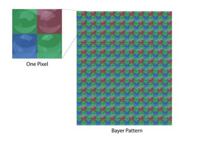
How a 2x2 pixel of photodetectors is arranged in a Bayer
Each photodetector is built on the silicon substrate and contains a photodiode to collect photons and three transistors: a row selector, an amplifier, and a reset transistor. The photodetector is topped by a color filter and a microlens that focuses light onto the photodiode.
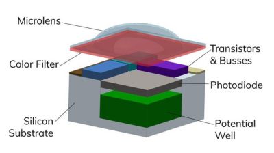
The geometry in a single photodetector
Each photodetector consists of the silicon substrate, a potential well, and a photodiode to measure the incoming photons. The color filter and microlens focus and filter the light, and the transistors and busses amplify and transmit the current produced.
This array of photodetectors is centered on a chip as the focal surface of a lens assembly. The array is also surrounded by analog and digital circuits used to assemble and output a digital image.
Design Considerations for a CMOS Image Sensor
A CMOS image sensor is a complex system that deals with physics on an atomic level all the way up to the mechanical requirements of packaging into a device assembly. Teams who are designing a new CMOS sensor should consider the following aspects:
Photonic Design
The behavior of the photodiode is critical to the performance of a CMOS sensor. Designers must consider photonics parameters, such as optical efficiency, quantum efficiency, dark current, and the electric charge generated. The design must also consider the wavelength of light being detected, from infrared to visible to ultraviolet.
Optical Design
The accuracy and efficiency of a CMOS image sensor depend on the quality of the image projected onto the sensor array. Optical engineers must develop an optimized lens assembly that delivers a clear, planner projection onto the surface. The effect of spatially-varying non-normal incident of light from the lens to the sensor surface should also be considered to obtain a more accurate sensor response. They also need to design the microlenses on top of each photosensor to deliver as much light as possible to the photodiode and understand the impact of incident light on the sensor.
Analog and Digital Circuit Design
One of the advantages of active-pixel sensors is the concept of having all the necessary analog and digital circuitry placed as an integrated circuit on the same chip as the sensor, creating a camera on a chip. Circuit designers need to take into account power issues, timing, signal integrity, and other considerations while fitting as many pixels as possible in as small a form factor as possible. They also need efficient analog-to-digital converters (ADC) and digital image processing capabilities on the chip itself.
Packaging
Once the chip is designed, it needs to be protected and provide connections to the electronics that will use the image. Packaging must address thermal, stress, and vibration issues while keeping costs down. Often the optical chip is packaged with other components that use or support the camera system.
The Future of CMOS Image Sensors
Improvements in semiconductor manufacturing technologies have a direct impact on image sensor capabilities. As feature size decreases, architects can fit more pixels into a smaller area. Consumers see this most commonly in the ever-increasing pixel count on their mobile phone camera while fitting in the same or smaller volume.
The speed of cameras using CMOS image sensors is also increasing. Another growth area is the proliferation of megapixel video cameras in automotive applications to give drivers more awareness of their surroundings and inform autonomous driving systems.
Experts predict more work on the digital image processing done on the sensor chip to produce an even better digital image. Work is also being done to look at different geometries for the photodiode, switching from red-green-blue (RGB) filters over the photodetectors to cyan-yellow-magenta (CYM) filters for greater sensitivity and a stronger electrical signal. Additional work is going into better low-light sensitivity and performance in near infrared (NIR) imaging.
Related Resources
Let’s Get Started
If you're facing engineering challenges, our team is here to assist. With a wealth of experience and a commitment to innovation, we invite you to reach out to us. Let's collaborate to turn your engineering obstacles into opportunities for growth and success. Contact us today to start the conversation.