ANSYS BLOG
April 19, 2021
224 Gbps or Bust: How Samtec Leverages Ansys HFSS for High-Speed Interconnect Design
“I need warp speed, Mr. Scott!” – James Tiberius Kirk
With that command – one of the most famous lines in “Star Trek” oeuvre – Montgomery Scott and the Engineering Department of NCC-1701 would fix the warp drive to save the crew. Although science fiction, the concept of warp speed illustrates the constant demand for faster data rates.
In today’s real world, the underpinning of global communications networks are the signal channels routing data at the fastest rates possible. Since summer of 2020, 224 Gbps channel data rates have been a reality. While years from production, the race is on to develop 224 Gbps semiconductor and high-speed interconnect solutions.
High-Speed Interconnect Design Challenges
As a provider of a wide ranges of high-performance and high-speed interconnect solutions, Samtec’s design engineers must optimize the entire signal path, not only the mated connector pair. As the illustration below shows, a signal path has many component parts: transceiver and receivers, die-to-packaging transitions, ball grid array (BGA) breakout regions, printed circit board (PCB) traces, connector breakout regions and the connector pairs themselves.
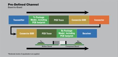
Components of typical 224 Gbps signal channel
In addition, several design details must be considered:
- What PCB laminate is best for a specific application?
- What PCB stack-up design makes the most sense?
- Which PCB trace types — mid-board strip lines or top/bottom layer microstrips — should be used?
- What connector pin-out makes sense?
Size is another design constraint. Form factors continue to decrease, so connector pitches are getting denser. Smaller pitches introduce their own concerns, such as crosstalk and insertion loss. This is primarily due to the proximity of one differential pair to the next, reduced space for routing, and a reduction in grounds pins.
As with any engineering decision, there are always tradeoffs. The slightest details affect signal channel and 224 Gbps interconnect performance. As an example, if the PCB laminate changes from MEGTRON 6 to MEGRTON7, that may decrease the dielectric constant (Dk). How does that affect overall signal channel and connector performance? It may help, or it may not.
Any number of design decisions affect multi-gigabit per second channel data rate performance. As a result, it's important to fine the right technical approach. Thankfully, state-of-the MCAD/ECAD software enables multiple design and simulations cycles for iterative product development and optimization.
Samtec + HFSS Optimize High-Speed Interconnect Designs
Samtec’s mechanical engineers first design next-gen interconnect solutions with industry standard MCAD tools. Designers conceptualize, create, validate and iterate complex 3D structures. This approach helps predict real-world physical behavior. The mechanical models port into ECAD tools like Ansys HFSS to analyze and optimize 3D structures with high-frequency electromagnetic fields.
The flexibility of the state-of the-art mesh solvers in Ansys HFSS allows Samtec to optimize high-performance interconnect designs. Like precision MCAD tools, adjusting component and channel wide models within HFSS leads to optimized performance.
What are some design variables that can be adjusted? Connector contact geometry — pin width and thickness, plastic width and thickness — can be simplified for improved signal path performance. Smaller pin lengths within the connectors minimize the distance the signal must travel. Engineers can optimize connector BORs. Material dielectric values — metal pins, PCB traces, vias and more – can all be adjusted on the fly.
As a design example, Samtec used Ansys HFSS to maximize signal integrity (SI) performance of the 0.80 mm NovaRay® Extreme Density Array product family. The flexibility of Ansys HFSS enabled analysis of multiple pinout types based on the desired result. The first pinout eased the design of the BOR. The second improved SI performance at higher data rates. Notice the illustrations below. Adjusting vias, PCB stack-up and other design features enables holistic channel data rates analysis.
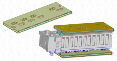
Ansys HFSS models of the Samtec NovaRay® Extreme Density Arrays
The accuracy of Ansys HFSS also enables improved interconnect product design. Solver accuracy can reach error levels well below manufacturing tolerance, which allows virtual prototyping. The first-in, first-out (FIFO) principle applies: Accurate design inputs lead to improved product designs.
From Samtec’s perspective, Ansys HFSS is a deterministic solver. Designs can handle small adjustments without starting from scratch each time. HFSS doesn’t blow up with a small change. These features and reliability help Samtec better understand the connector design process. Design input adjustments minimize output anomalies.
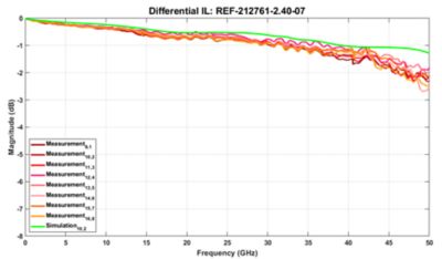
Samtec considers HFSS to be a benchmark 3D EM solver. Engineers can depend on HFSS outputs. As a result, Samtec leverages HFSS accuracy to offer predictable correlation to measurements at frequencies up to 110 GHz. Notice the correlation between measured and simulated differential insertion loss (IL) on the Samtec NovaRay® SI Evaluation Kit. The IL < 3db at > 50 GHz lends credence that NovaRay offers a path to 224 Gbps operation.
The combination of Samtec’s design techniques and flexibility and accuracy of the Ansys HFSS prove 224 Gbps interconnect solutions are just around the corner. Warp speed, indeed.
To learn more about interconnect product design workflow, view the recorded webinar: Practical Ports for Perfect Performance.