Synopsys and Ansys power the future of innovation—connecting silicon to systems.
ANSYS ADVANTAGE MAGAZINE
DATE: 2020
Elastic Compute & Big Data Analytics Tackle Physical Verification Complexity
By Nitin Navale, CAD Manager, Xilinx, San Jose, U.S.A.

Larger, more complex silicon designs are straining verification methodologies and slowing time to results and time to market. Xilinx engineers wanted to leverage big-data analytics to simplify their verification flow on leading-edge chips, and they looked to Ansys for answers.
Many of today’s rapidly evolving applications — be they in artificial intelligence, autonomous vehicles, infrastructure or high-performance computing (HPC) — rely on leading-edge field-programmable gate arrays (FPGAs) for their performance and flexibility.

The Xilinx XCVU440 can contain up to 400 fabric sub-region (FSR) instances, each with up to 5,000 IP block instances.
Silicon design trends — and their attendant pressures for more performance and functionality — flow back upstream to engineers at Xilinx, the venerable 35-year-old Silicon Valley company that invented field programmability. Owing to their unique programmable architecture, FPGAs have always been relatively larger devices than standard integrated circuits or custom systems-on-chips (SoCs), and lately the explosion of new features on the company’s Versal ACAP products has only made them larger and more complex.
Further, ultra-low voltages lead to razor-thin noise margins, so variability can be severe. This affects timing, where the timing delay variation as a function of voltage is changing with each node.
With billions of instances and transistors, these FPGA designs require higher capacity and enough scale and coverage (50x more than the traditional approaches to dynamic analysis and static signoff) for proper timing analysis. If tool capacity is already limited, teams usually aren’t in a budget or time-to-market position to afford running longer simulations or more simulation cycles to get proper coverage.
Other issues to consider include the complexities of 2.5D and 3D package routing and techniques such as chip-on-wafer-on-substrate (CoWoS), aging-induced stresses on fin field-effect transistors (FinFETs), as well as thermal and Joule heating. Additionally, designers need to model the chip, package and system together to ensure a sound overall power delivery network.
Wrestling With Complexity
Confronted with this kind of complexity, the team at Xilinx has adapted to take on these verification challenges. The company has embraced big data analytics and elastic compute functionality, powered by Ansys, which speed the designs to completion while accurately covering multiphysics issues that can vary significantly on chip.
One of the company’s newest products is the Xilinx XCVU440, which contains 30 million ASIC gates. Any product from this family can contain up to 400 fabric sub-region (FSR) instances, each with up to 5,000 IP block instances. (An FSR is the next-largest building block below the full chip.) The IP blocks are heterogeneous in nature — custom, semi-custom, digital and mixed signal.
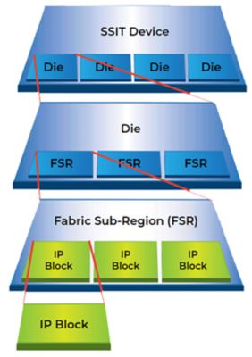
Silicon interconnect technology devices contain multiple dies on a silicon interposer. A single die can contain between 100 and 400 fabric sub-region (FSR) instances. The FSR typically has 2,500 to 5,000 instances of IP blocks.
Xilinx has no shortage of experience with static timing analysis (STA), but modern STA is becoming an increasing challenge with greater feature complexity at finer process nodes. The company needed accurate modeling for supply voltage and wider coverage. With billions of instances and transistors on a single die, engineers needed higher capacity from a solution that can scale with enough coverage.
Traditionally, to perform STA on a sub-region, the designer would load the entire chip into the tool and black-box regions that didn’t need their attention. But it’s proving more and more difficult to isolate or prune parts of the design to do STA, and scaling with traditional methods has started to break down. And even black-boxed IPs can consume memory and affect tool performance! The traditional approach works best for large blocks that have few instances, and XCVU440 is just not that kind of beast.
Instead, the team investigated a subsystem approach that would simplify the STA challenge and speed time to results without compromising accuracy. They chose to leverage Ansys SeaScape, a purpose-built big data platform that delivers elastic compute functionality and distributed file/data service. SeaScape can handle large designs and distribute them efficiently across the compute farm on smaller CPUs with smaller memory footprints. From this platform, they were able to load the chip and prune it down to create a virtual design for STA analysis that was composed of only the most relevant aspects of the full device.
With simulation data sizes growing to unmanageable dimensions, Xilinx leveraged Ansys SeaScape and its map-reduce analytics to prune chip-scale designs for faster timing analysis.
Xilinx has an internal process called Timing Capture, which requires not just a physical view of the chip, but also awareness of its point-to-point interconnect delays. Instead of timing for the whole design, Timing Capture focuses on a subset of highly critical interconnect paths.
Using Ansys Seascape for large design Scaling For Timing Analysis
The design team started by loading the entire chip into SeaScape as an abstracted physical view — DEF and SPEF (Design Exchange Format, Standard Parasitic Exchange Format) for chip-level blocks and LEF (Library Exchange Format) for IP blocks — and pruned it down to contain only the precise list of IP instances desired for that downstream analysis. Within SeaScape, they could easily delete unwanted IP instances, then delete any nets that were left floating. To ensure no capacitive loading is lost, all dangling coupling caps were attached to a virtual aggressor. The final view is reduced in scope from the original chip, containing the precise IP instances needed for analysis with no loss of accuracy.
From there the team could export pruned Verilog, DEF and SPEF views that could be loaded into other analyses.
With simulation data sizes growing to unmanageable dimensions, Xilinx leveraged Ansys SeaScape and its map-reduce analytics to prune chip-scale designs for faster timing analysis.
Xilinx ran an experiment using a single FSR on a “mini-SoC,” containing roughly 375,000 block instances. Had the team not filtered it, but run the pure FSR as is, their STA timer wouldn’t have been able to handle its size. The pruning job, which Ansys SeaScape manages seamlessly, required only 40 SeaScape workers and yielded a 6.5-hour runtime. STA is then able to handle the pruned design in a very respectable 12 hours per corner (wall clock time). Interestingly, pushing the same design through Ansys Path FX yielded a runtime of only one hour per corner (using one master license and 42 workers).
The team then ran the same test on a medium-sized multi-FSR experiment (33 FSRs and 32 million block instances). As before, STA could not finish on the unpruned design. After pruning, STA is now finishing with a wall clock time of four days per corner. Once again, Path FX is still faster with a one-day turnaround.
What the team accomplished was to take a near full-chip version of the design, prune it down to fit inside their STA tool, and achieve signoff in a reasonable amount of time.
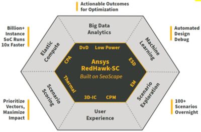
Ansys RedHawk-SC: Future-Friendly Full-Chip EM/IR SignOff
In parallel with this effort, another Xilinx team was using Ansys RedHawk-SC for EM/IR signoff to see how that tool handles complexity and scale on the same full-chip scale. The goal with EM/IR signoff is to partition the chip into something that can be handled on a 1–2 TB host and run overnight, preferably in under eight hours.
To better grasp the increase in design complexity at later technology nodes, Xilinx’s 16 nm UltraScale+ design can be used as a point of reference. The team signed off EM/IR for that entire chip by dividing it into seven partitions, which took about one person-month for initial setup. Iterative reruns with ECOs consumed roughly one person-week to cover the whole chip. To achieve the same tool capacity and analysis throughput, the 7 nm Versal chip required 40 partitions and 5x the engineering person-hours to finish along the same timeline. That sort of resource investment simply cannot scale into the future.
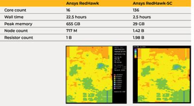
But unlike with STA, this time Xilinx engineers were able to feed the unpruned data set directly into RedHawk-SC, which is built on top of SeaScape and thus handles the pruning natively. In the experiment, the team analyzed a medium-sized place-and-route block for static IR drop (the DC voltage that is lost across the power delivery network due to its electrical resistance), comparing a four-core classic RedHawk run against a 16-core RedHawk-SC run. The test case saw 57-minute wall clock times with classic RedHawk compared to 18 minutes for RedHawk-SC, which is a good baseline for additional comparisons. The next comparison tested a very large place-and-route region containing 78 million logic gates — once again running static IR drop in both tools. Classic RedHawk maxed out at 16 cores on a single host, while RedHawk-SC comfortably scaled up to 136 cores across the LSF farm.
Because RedHawk-SC is partitioning the design across so many machines or workers, the experiment required only 29 GB of peak memory per worker, versus 655 GB peak memory with classic RedHawk. Comparing wall clock times, RedHawk-SC’s distributed compute finished the static analysis in a mere 2.5 hours, compared to 22 hours for classic RedHawk.
The result was a noteworthy improvement in performance. RedHawk-SC is enabling faster turnaround and distributed compute, and it’s doing so with finer granularity than classic RedHawk. There’s no doubt: This is the future of EM/IR analysis.
ANSYS Path FX: Elastic Compute On Chip-Scale Interconnect Delays
In addition to traditional STA Timing Closure, Xilinx has an internal process called Timing Capture, which is specific to its all-programmable architecture and is driven by the company’s Vivado software. Vivado is the tool that programs the chip and is like a full implementation flow unto itself. Timing Capture requires not just a physical view of the chip, but also awareness of its point-to-point interconnect delays.
Because it would be impractical to calculate these delays while programming the chip, Xilinx instead pre-calculates them while designing the chip and then programs the delays into Vivado. The tool is thus already aware of interconnect timing at various PVT corners and uses that timing to optimize the chip during programming. The process for measuring these delays is similar to critical path timing analysis in traditional STA. Instead of timing for the whole design, Timing Capture focuses on a subset of highly critical interconnect paths outlined by Vivado.
For a traditional STA tool, every conflicting path must be handled separately. Each conflict means a separate call to update timing. Even for paths that can be grouped together, the process is time-consuming. Xilinx wanted better throughput and parallelism without sacrificing accuracy.
The team turned to Ansys Path FX for critical path timing analysis, which can calculate pin-to-pin delays simultaneously across the entire chip — even on conflicting paths. Ansys Path FX accomplishes this feat by applying constraints to each path independently and then distributing the many paths across many workers fully in parallel.
Xilinx Versal is an adaptive compute acceleration platform (ACAP), a new category of heterogeneous compute devices.
Delay calculations based on the FX transistor-level simulation model mean no accuracy loss.
This is where elastic compute comes into play: You can farm out all these paths as small jobs to many hosts across your LSF (load-sharing facility) farm.
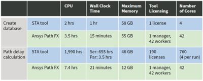
The team ran a head-to-head test comparing the performance of Path FX versus their traditional STA signoff tool on 95,000 query paths. In the test, creating the database took one hour of wall clock time in the company’s trusted STA tool, but only 15 minutes in Path FX with similar memory footprints (~55 GB).
The next stage — path delay calculation — is where Path FX really shined. The incumbent STA tool required 190 separate tool invocations and nearly 2,000 compute hours to finish measuring all paths. Wall clock time is difficult to precisely nail down, because the team employed many tool invocations running in a semi-parallel LSF configuration. In the best (and most expensive) case of running all 190 tool invocations fully in parallel, the best possible wall clock time would be 3.5 hours. More realistically, it was likely closer to 100 hours. Meanwhile, Path FX’s native parallelism allowed it to complete the same task with a single tool invocation and a mere 7.4 compute hours. Wall clock time for Path FX was a very crisp 21 minutes.
The results greatly exceeded the design team’s expectations. With the team’s semi-parallel approach using the traditional STA tool, they’d grown accustomed to this work taking a week.
Path FX’s configuration (one license and 42 workers) comes out looking more cost-effective than 190 licenses of the traditional STA tool.
Big, Fast And Accurate
To break through modern simulation bottlenecks, Xilinx has rethought its design methodologies and embraced new approaches using Ansys tools. These tools have proven they can dramatically speed up time to results without sacrificing accuracy when it comes to timing and EM/IR analysis. In doing so, Xilinx has embraced an approach already championed by companies such as Twitter and Amazon: big data analysis.
With simulation data sizes growing to unmanageable dimensions, Xilinx leveraged Ansys SeaScape and its map-reduce analytics to prune chip-scale designs for faster timing analysis. Similarly, RedHawk-SC and Path FX use intelligent pruning and partitioning, coupled with elastic big data compute, to break down each mammoth EM/IR or interconnect timing job into a stack of bite-size chunks. In all aspects of back-end analysis, the next generation of silicon will be relying on Ansys tools to make it out the door.