Synopsys and Ansys power the future of innovation—connecting silicon to systems.
TOPIC DETAILS
What is Inverse Design?
Inverse design is a computational approach to engineering that flips the conventional process around to offer a more optimal design and efficient approach to simulating materials design and nanofabricated platforms.
Conventional design approaches start with an existing solution and then use trial and error, both experimentally and in simulation, to meet enhanced specifications. This often involves going through multiple iterations and may become impossible to do rigorously when incorporating hundreds of design parameters.
On the other hand, inverse design looks at the desired performance of a system and uses mathematics to determine how to improve upon it. Engineers then use this mathematical toolbox, along with advanced optimization algorithms, to improve upon materials design, material properties, structure, and composition for any technology system and application. This process requires assessing the performance of the system, as well as high-resolution measurements of what is physically happening in the system, to make these decisions.
Inverse design generally refers to the paradigm shift of starting with specifications and automating the iteration process. It can come in different flavors and has applications in a wide range of applications. It is a powerful tool in applications where the performance is very sensitive to the morphology and material properties of the device, which is the case for structures with advanced materials and very high-frequency electromagnetics applications. Furthermore, given that these are emerging technologies and processes, inverse design provides a powerful tool to rapidly find solutions where none yet exist.
Because of this, inverse design approaches are valuable in nanophotonics applications, such as photonic integrated circuits (PICs), optoelectronics, metamaterials, and metasurfaces.
Fundamentals of Inverse Design
Inverse design is essentially an advanced reverse engineering optimization problem. While inverse design refers to the overall methodology, it is underpinned by machine learning and deep learning optimization. It offers a way to compute complex material systems more efficiently than conventional methods that don’t always have the computational power, dataset, and learning model to solve complex problems.
The overall inverse design process first defines the problem before searching for optimal solutions. It is a complicated process, incorporating highly complex elements, such as calculating derivatives, and has a high learning curve because it is still a relatively new approach. However, once mastered, it provides a lot more design space for developing different and more complex design variations.
Users have many choices on how to address certain design problems based on the desired performance metrics, including optimizing an existing device by parameterizing it, reducing the footprint of the device, opening new degrees of freedom to improve the device, or creating completely new systems. Beyond device performance itself, inverse design can be used to make technology designs robust against manufacturing tolerances.
Photonics Applications of Inverse Design
For photonics devices specifically, photonic inverse design (PID) is used. In this process, the materials of choice are specified at the beginning of the process. It modulates the arrangement of the materials — that is, the removal and addition of materials in specific locations across the optimization region of the device and through user-defined shapes or pixelated topology.
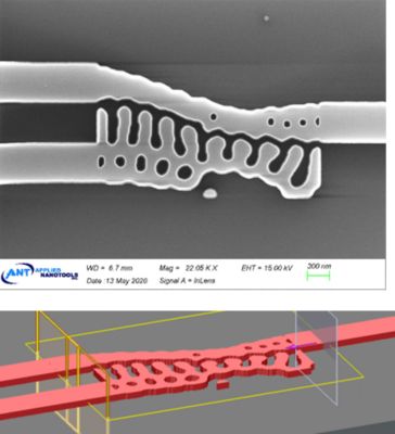
Topology-optimized geometry of a 50/50 waveguide splitter in Ansys Lumerical software (below) after photonic inverse design (PID) and an SEM image of the same device manufactured by Applied Nanotools on the SOI platform using e-beam lithography
There are a lot of areas in the photonics space, especially PICs, where inverse design can be used to construct advanced photonic components. Some key examples of using inverse design in advanced photonics include:
- Splitters that split a photonic channel (optical waveguide) into two channels
- Couplers that transfer light between channels
- Polarization-splitting grating couplers that perform routing and coupling functions
- Filters, including topological color filters for routing light into different channels on PICs
- Photonic metamaterials and metasurfaces
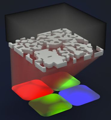
This optimization exploits novel patterning to physically sort RGB light into the various subpixels, helping achieve higher SNR ratios and avoiding additional materials in the nanofabrication process.
Advantages and Limitations of Inverse Design
Inverse design is a process that can be highly beneficial under the right circumstances, but it’s still a relatively new approach, and it’s not always needed based on the intended performance, functionality, tolerances, and complexity of the system being designed. Here are some advantages and limitations of inverse design methods today.
Advantages of Inverse Design
- Offers a high-performance tool that efficiently develops unintuitive designs
- Creates devices with more degrees of freedom (up to thousands of degrees of freedom) that wouldn’t be possible with conventional parameters
- Reduces the need for prototyping and physical experimentation in early development stages
- Accelerates discovery of materials
- Improves device performance without multiple iteration steps (including multiple simulation stages)
- Provides an ideal solution for photonics applications, where the state-of-the-art devices don’t have years of developmental knowledge compared with conventional electronics
- Offers an efficient way to discover new knowledge, mechanisms, and material optimization in emerging technology applications
Limitations of Inverse Design
- Has a steep learning curve, even for experienced engineers, so it is not as widely used as it could be
- Uses a lot of Python modules and optimization frameworks that require experience in those computer science domains
- Requires lots of coding experience as the sensitivity to conditions differs for both existing and new devices
- Increases computational costs
- Requires some fine-tuning of devices at the end to make sure they are physically feasible and not just theoretically ideal devices
The Role of Simulation in Inverse Design
Simulation software is a key part of inverse design. While inverse design wouldn’t be possible without advanced simulation software, the only simulation packages that currently support inverse design are those based on finite-difference time-domain (FDTD), such as Ansys Lumerical FDTD advanced 3D electromagnetic FDTD simulation software. This is because a lot of information about the physics of the material system is required (due to the large number of material and system factors) to perform inverse design approaches.
FDTD-based simulation is also a gold standard in photonics, but it is computationally expensive, so this is currently where a lot of the computational cost of inverse design arises. The other computational aspect is the gradient-based calculations, which can also take time to perform. Even though computational time can be a lot for FDTD, it is still cheaper than the time of an engineer, who has to go through physical prototyping stages and will take a lot longer to achieve the same results.
The inverse design methodology is a complex framework process around the FDTD simulation, so without FDTD, inverse design would not be possible. For many applications and devices, FDTD will be enough. But for high-performance applications where the performance needs to be improved to the maximum capabilities possible or for applications where researchers are trying to push the limits of what they can do in a given footprint, inverse design is a highly beneficial approach.
Emerging Trends in Inverse Design
Inverse design is still a relatively new approach in the simulation, photonics, and advanced technology spaces, so there continues to be a lot of changes about how inverse design problems are tackled and what applications inverse design is used in.
Inverse design continues to be integrated with different artificial intelligence (AI) algorithms, including machine learning, deep learning, and deep neural networks. This integration is intended to improve the capabilities of inverse design methods, including automating the gradient descent calculations.
Interest is growing in having full control over the performance metrics. Improvements and automation in this area will enable researchers to have full control over defining the performance metrics that they're interested in. Currently, inverse design can be used to look at the performance of photonic systems, but is constrained to how much power is in each mode or port. However, there is a push to achieve more advanced performance optimizations too, such as optimizing light intensity in certain regions or optimizing for phase delays between modes.
A lot of progress has been made toward optimizing different problems, but there are still many more performance metrics that can be targeted with inverse design that are being considered. There’s also a drive to try to make the methodology more customizable and easier to use so it can be adopted by a wider range of industries in the coming years.
If you’d like to learn more about performing inverse design simulation methods on your products, get in touch with our technical team and find out how Ansys, part of Synopsys, can help make the process easier for you.
Related Resources
现在就开始行动吧!
如果您面临工程方面的挑战,我们的团队将随时为您提供帮助。我们拥有丰富的经验并秉持创新承诺,期待与您联系。让我们携手合作,将您的工程挑战转化为价值增长和成功的机遇。欢迎立即联系我们进行交流。