ANSYS BLOG
July 7, 2021
The Next HFSS Game Changer: Phi Plus Mesher for Bondwire and MCAD Layout Assemblies
Electronics engineers are striving to design more functional chips, printed circuit boards (PCBs) and products with increasingly demanding specifications, all while shrinking form factors. The result is massive, unprecedented design complexity with more components being placed in closer proximity and coupling electromagnetically, intentionally or otherwise. However, complexity isn’t the only issue faced by the electronics industry.
Opportunities in the burgeoning 5G, autonomy and industrial internet of things (IIoT) markets are driving designers to not only focus on innovation, but to launch those same innovations quickly to capture the market. But market conditions present their own challenges. Case in point: the global shortage of chips for automotive technologies, which has already reached main street where your neighborhood automotive dealers are scrambling to maintain inventory for the summer.
Ansys has met engineers’ need for speed by delivering a number of breakthroughs for Ansys HFSS 3D high-frequency electromagnetic simulation software. Recent highlights include an elastic solver technology that allows a single HFSS simulation to be solved on multiple machines; HFSS being enabled on Ansys Cloud hosted by Microsoft Azure; a dedicated, layout-based workflow for HFSS called HFSS 3D Layout; and HFSS Mesh Fusion, which was introduced earlier this year in Ansys 2021R1. All these enhancements allow HFSS users to solve at scale, and solve larger and more complex designs faster with the accuracy, rigor and reliability of Ansys HFSS.
Phi Plus Mesher Delivers More Speed and Capacity
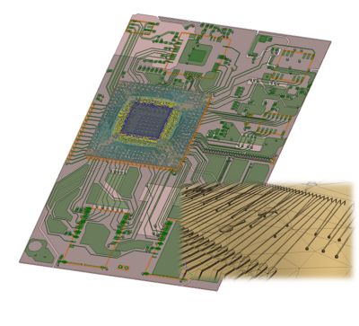
Now, to address the demanding needs of HFSS users, we’re introducing the Phi Plus mesher with the upcoming release of Ansys 2021R2. It’s another breakthrough technology for HFSS. This new meshing technology in the HFSS 3D Layout workflow will deliver more speed and capacity to the HFSS solution process, enabling HFSS users to solve the most complex designs. This high-performance computing (HPC) enabled, computer-aided-design (CAD) aware meshing technology uses local knowledge of the geometry – such as the layered media of a PCB or IC package, 3D components like a connector or a surface mount capacitor, and bondwires – to perform locally optimized meshing techniques for those geometries. For bondwires in particular, the upfront knowledge of their geometry (a cylindrical cross section swept along a line), aids the Phi Plus mesher in efficient creation of the bondwire’s mesh along with minimizing the required number of elements and improving their overall quality. With these advanced techniques and the fact that this meshing technology is built from the ground-up for parallelization, the end result is a much faster initial mesh generation than before.
A recent benchmark on a PCB plus bondwire package model (image below) showed that initial mesh generation was 18x faster than previous generation bondwire meshing technology, bringing the initial mesh time down to a matter of minutes. Across a broad range of geometries over 50 models, the Phi Plus mesher averaged an almost 11x improvement in initial mesh times. In addition, on average, the overall mesh was smaller in size while being higher quality, which also benefits solver run times.
Following on the 2021 R1 heels of HFSS Mesh Fusion, the new Phi Plus mesher will be yet another game changing technology delivered by the Ansys HFSS development team. To learn more about this new feature, along with the other new features of HFSS 2021 R2, view our on-demand webinar: Ansys 2021 R2: Ansys HFSS Update.