-
-
Accédez au logiciel étudiant gratuit
Ansys donne les moyens à la prochaine génération d'ingénieurs
Les étudiants ont accès gratuitement à un logiciel de simulation de classe mondiale.
-
Connectez-vous avec Ansys maintenant !
Concevez votre avenir
Connectez-vous à Ansys pour découvrir comment la simulation peut alimenter votre prochaine percée.
Pays et régions
Espace client
Support
Communautés partenaires
Contacter le service commercial
Pour les États-Unis et le Canada
S'inscrire
Essais gratuits
Produits & Services
Apprendre
À propos d'Ansys
Back
Produits & Services
Back
Apprendre
Ansys donne les moyens à la prochaine génération d'ingénieurs
Les étudiants ont accès gratuitement à un logiciel de simulation de classe mondiale.
Back
À propos d'Ansys
Concevez votre avenir
Connectez-vous à Ansys pour découvrir comment la simulation peut alimenter votre prochaine percée.
Espace client
Support
Communautés partenaires
Contacter le service commercial
Pour les États-Unis et le Canada
S'inscrire
Essais gratuits
ANSYS BLOG
November 1, 2022
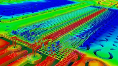
The Challenge of Electromagnetic Modeling and Simulation for Silicon Interposers in 2.5D/3D-IC Chip Designs
The use of 2.5D/3D-IC packaging technology has re-energized the microchip industry — particularly at the high end, such as central processing units (CPUs), graphics processing units (GPUs), and systems-on-chip (SoCs) — bypassing the diminishing returns of process node advancements in ultra-deep submicron. But the packaging technology is complex and its ramifications echo across design teams, from chip design to package and printed circuit board (PCB) development.
These development teams have different requirements and needs. The chip team needs tools that support modeling and simulation for electromagnetics, timing, power, thermal effects, and mechanical effects. The interactions of these phenomena also need to be captured, effectively expanding the requirement to a set of tools that support multiphysics simulation. This tool set will be applied to each chiplet and the overall dynamically interactive architecture of the multichip 2.5D/3D-IC design.
PCB and package developer tool requirements are quite similar but decidedly more expansive. Their modeling and simulation tools need to secure electromagnetics, power and signal integrity, thermal, and mechanical aspects of package and board designs, both individually and from a multiphysics frame of reference. However, engineers also have to account for multiphysics interactions between the board, package, and chip as a complete system.
Nested within all the design and simulation necessities is the interposer that separates chiplets — or stacks of chiplets in a full 3D-IC design — from the substrate in a 2.5D/3D-IC package. Interposers physically separate die in the horizontal plane while providing paths for routing chiplet stack power and signaling paths to the ball grid array (BGA) of the package.
The Advantages of Silicon Interposers
An increasingly popular choice for the material composing this element is silicon. Silicon interposers are built using IC manufacturing processes and, despite typically being more expensive, can offer distinct advantages. One is the thermal expansion coefficient of the material, which will match that of the die it’s in contact with. Another is the arrangement of through-silicon vias (TSVs) that the interposer can support. The array can be both dense and well aligned with the ball pitch of BGA packaging. Furthermore, the silicon will support fine pitches for traces used in signal and power distribution. Together, these capabilities provide significant performance benefits in terms of raw speed and bandwidth.
But all of these densely packed features in a silicon interposer offer additional problems to the members of the teams designing 2.5D/3D-IC chips, packages, and boards. The modeling and simulation support for a silicon interposer is a major challenge — you can see there’s a lot going on. Moreover, the silicon interposer is yet another complex component in a system of functions and capabilities that are all interrelated from a multiphysics perspective.
The concerns of 2.5D3/D-IC designers using silicon interposers include:
- Accuracy: Can an electromagnetic simulator capture all the details of my silicon interposer accurately?
- Run time: Will the simulation converge on an accurate and optimal solution to my interposer design parameters in a time of relevance, such as minutes or hours?
- Multiphysics: Can other physical factors such as mechanical and thermal phenomena, which can affect the interposer electromagnetic (EM) simulation, be included to provide a full multiphysics solution?
- System simulation: Can my interposer EM simulation be combined with work at the chip, package, and PCB level and still produce accurate, timely simulations at a system level?
- Comprehensive methodology: Is there a workflow or methodology for the tool set that can execute all of the above?
These and more questions were answered by Ansys at the “Comprehensive Multiphysics Analysis Platform for 3D-IC Interposers” webinar, held the first week of November. This webinar launched an extended series of webinar discussions on 3D-IC modeling and simulation, scaling from the chip level up to full PCB implementations. The presentation on November 3 set the stage by outlining the power integrity, thermal integrity, and signal integrity challenges of 3D-IC design and presented Ansys Redhawk-SC Electrothermal, a comprehensive multiphysics simulation solution for the problem set, using interposer design as an illustrative application example.
View the on demand webinar now to learn all about the challenges and solutions of 3D-IC design.